Programming method for NAND EEPROM

a programming method and eeprom technology, applied in the field of memory devices, can solve the problems of non-volatile memory cells, loss of whatever data was in rams, cost of a generally slower access rate and programming complexity, etc., and achieve the effect of higher/lower word line resistance and/or capacitive coupling ratio

Active Publication Date: 2007-03-01
MICRON TECH INC
View PDF16 Cites 216 Cited by
  • Summary
  • Abstract
  • Description
  • Claims
  • Application Information

AI Technical Summary

Benefits of technology

The various embodiments relate to non-volatile memory devices wherein differing word line pass voltages (Vpass) are utilized in the programming of non-volatile memory cells (such as floating gate or floating node/charge trapping memory cells) of NAND architecture EEPROM and Flash memory arrays, where the level of Vpass utilized is selected based on the position of the memory cell selected to be programmed in the memory string. In one embodiment of the present invention, the differing word line pass voltages (Vpass) are utilized depending on the placement of the memory cell being programmed in the NAND memory cell string. In another embodiment of the present invention, the differing word line pass voltages (Vpass) are utilized at the same time to compensate for faster and slower programming word lines/memory cells. In another embodiment, different word line pass voltages (Vpass) are applied to the string based on physical aspects of the word lines of the array, including, but not limited to, an interlaced array of alternating wide/thin cross section word lines which have higher/lower word line resistances and/or capacitive coupling ratios with the underlying non-volatile memory cells.
For one embodiment, the invention provides a method of programming memory ce

Problems solved by technology

Most RAM is volatile, which means that it requires a steady flow of electricity to maintain its contents.
As soon as the power is turned off, whatever data was in RAM is lost.
This allows a NAND array architecture to have a higher memory cell density than a comparable NOR array, but with the cost of a generally slower access rate and programming complexity.
A problem in programming NAND architecture Flash memory devices is that the non-volatile memory cells coupled to the different word lines of a given NAND memory string can have faster or slower programming characteristics dependent on their position in the memory st

Method used


Image

  • Programming method for NAND EEPROM
  • Programming method for NAND EEPROM
  • Programming method for NAND EEPROM

Examples


Embodiment Construction

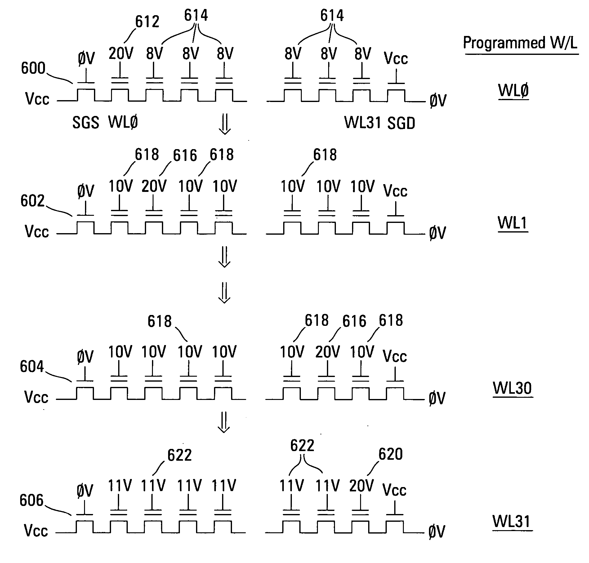
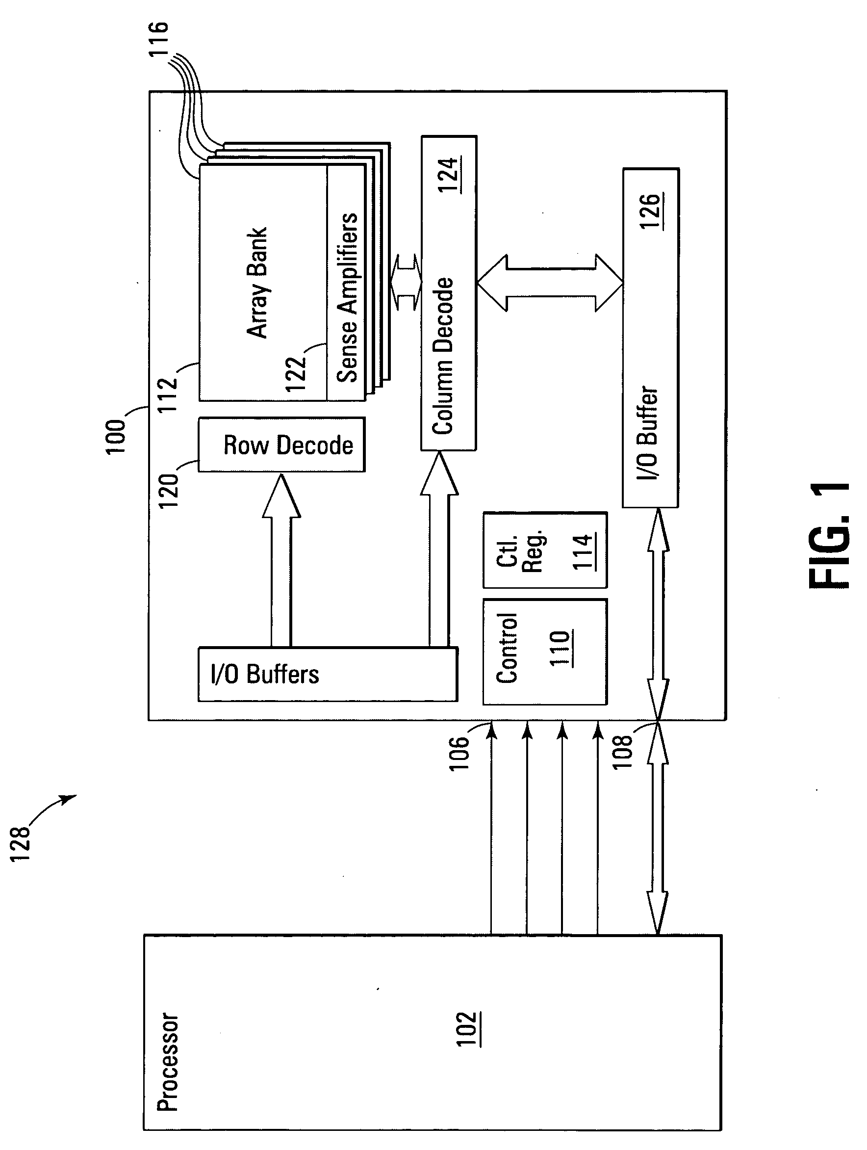
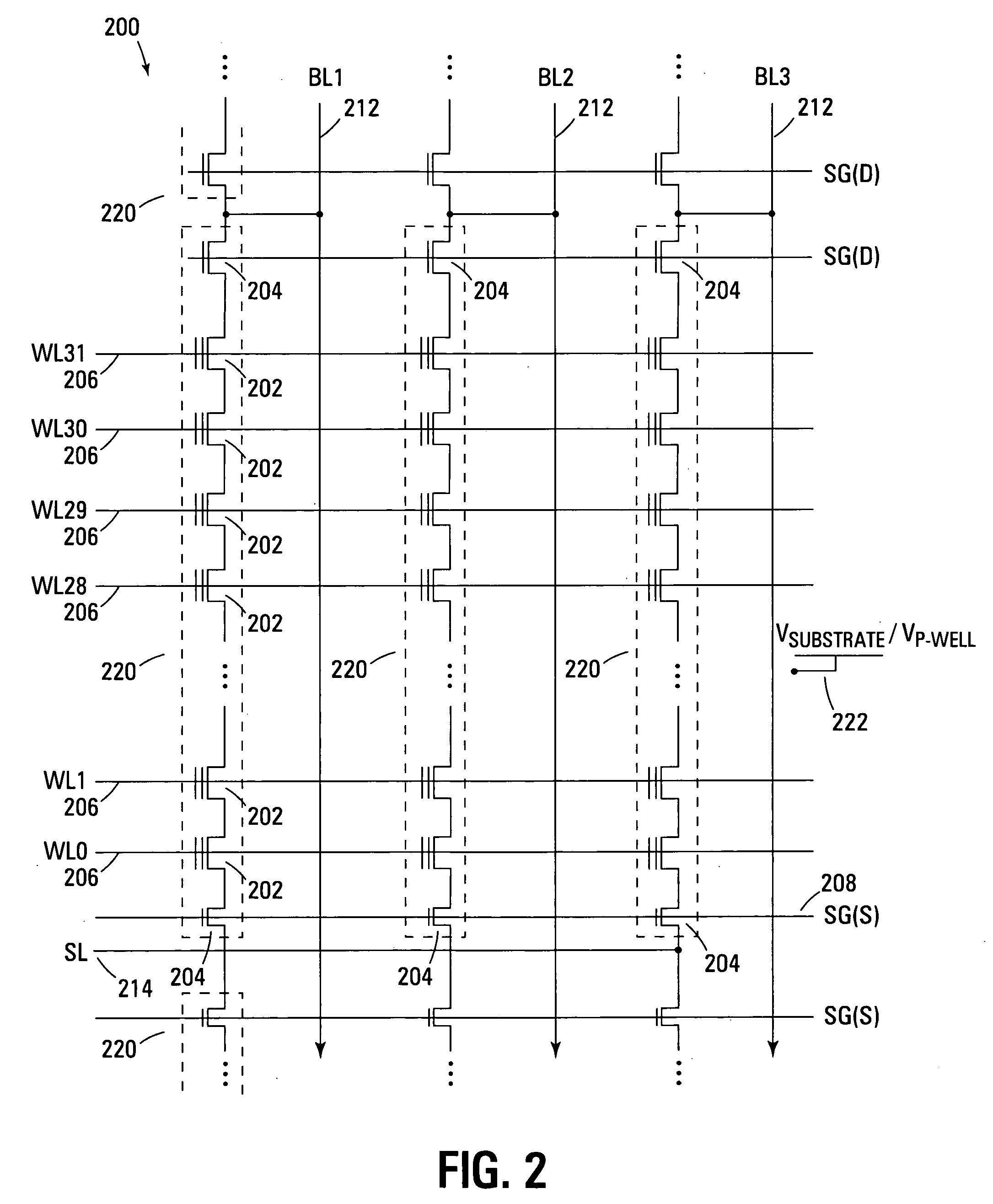
In the following detailed description of the preferred embodiments, reference is made to the accompanying drawings that form a part hereof, and in which is shown by way of illustration specific preferred embodiments in which the inventions may be practiced. These embodiments are described in sufficient detail to enable those skilled in the art to practice the invention, and it is to be understood that other embodiments may be utilized and that logical, mechanical and electrical changes may be made without departing from the spirit and scope of the present invention. The terms wafer or substrate used in the following description include any base semiconductor structure. Both are to be understood as including silicon-on-sapphire (SOS) technology, silicon-on-insulator (SOI) technology, thin film transistor (TFT) technology, doped and undoped semiconductors, epitaxial layers of a silicon supported by a base semiconductor structure, as well as other semiconductor structures well known t...


PUM


Abstract

A NAND architecture non-volatile memory device and programming process is described that programs the various cells of strings of non-volatile memory cells by the application of differing word line pass voltages (Vpass) to the unselected word lines of the memory cell string or array during an programming cycle. In one embodiment of the present invention, the differing word line pass voltages (Vpass) are utilized depending on the placement of the memory cell in the NAND memory cell string. In another embodiment of the present invention, the differing word line pass voltages (Vpass) are utilized to compensate for faster and slower programming word lines/memory cells.

Description

TECHNICAL FIELD OF THE INVENTION The present invention relates generally to memory devices and in particular the present invention relates to EEPROM and Flash memory devices. BACKGROUND OF THE INVENTION Memory devices are typically provided as internal storage areas in the computer. The term memory identifies data storage that comes in the form of integrated circuit chips. There are several different types of memory used in modern electronics, one common type is RAM (random-access memory). RAM is characteristically found in use as main memory in a computer environment. RAM refers to read and write memory; that is, you can both write data into RAM and read data from RAM. This is in contrast to ROM, which permits you only to read data. Most RAM is volatile, which means that it requires a steady flow of electricity to maintain its contents. As soon as the power is turned off, whatever data was in RAM is lost. Computers almost always contain a small amount of read-only memory (ROM) t...

Claims


Application Information

Patent Timeline
IPC IPC(8): G11C16/04
CPCG11C16/0483G11C16/3427G11C16/12
Inventor GODA, AKIRAARITOME, SEIICHIMARQUART, TODD
Owner MICRON TECH INC
Why Eureka
Try Eureka