
Manufacturing method of optical disk and its manufacturing apparatus

a manufacturing apparatus and optical disk technology, applied in the field of manufacturing methods of optical disks and their manufacturing apparatus, can solve the problems of difficult to stably provide high-quality optical disks, difficult to suppress etc., and achieve the effect of suppressing the generation of bubbles

Inactive Publication Date: 2007-03-01
SONY CORP
View PDF6 Cites 3 Cited by
  • Summary
  • Abstract
  • Description
  • Claims
  • Application Information

AI Technical Summary

Benefits of technology

The present invention provides a manufacturing method and apparatus for optical disks that can stably produce high-quality disks without bubbles. The method involves coating a resin layer onto a substrate, arranging the substrate and a stamper in a chamber, and setting the chamber into an almost vacuum state. The substrate and stamper are then overlaid and pressed together, transferring the concave / convex portions of the stamper to the resin layer. This method can effectively suppress bubble generation and ensure the quality of the optical disk.

Problems solved by technology

However, in the adhering method in the vacuum, since the operation of the stamper which can suppress the generation of the bubbles as shown in FIG. 16A occurs accidentally and lacks reproducibility, it is difficult to certainly suppress the generation of the bubbles and it is difficult to stably provide the optical disks of high quality.

Method used


Image

  • Manufacturing method of optical disk and its manufacturing apparatus
  • Manufacturing method of optical disk and its manufacturing apparatus
  • Manufacturing method of optical disk and its manufacturing apparatus

Examples


Embodiment Construction

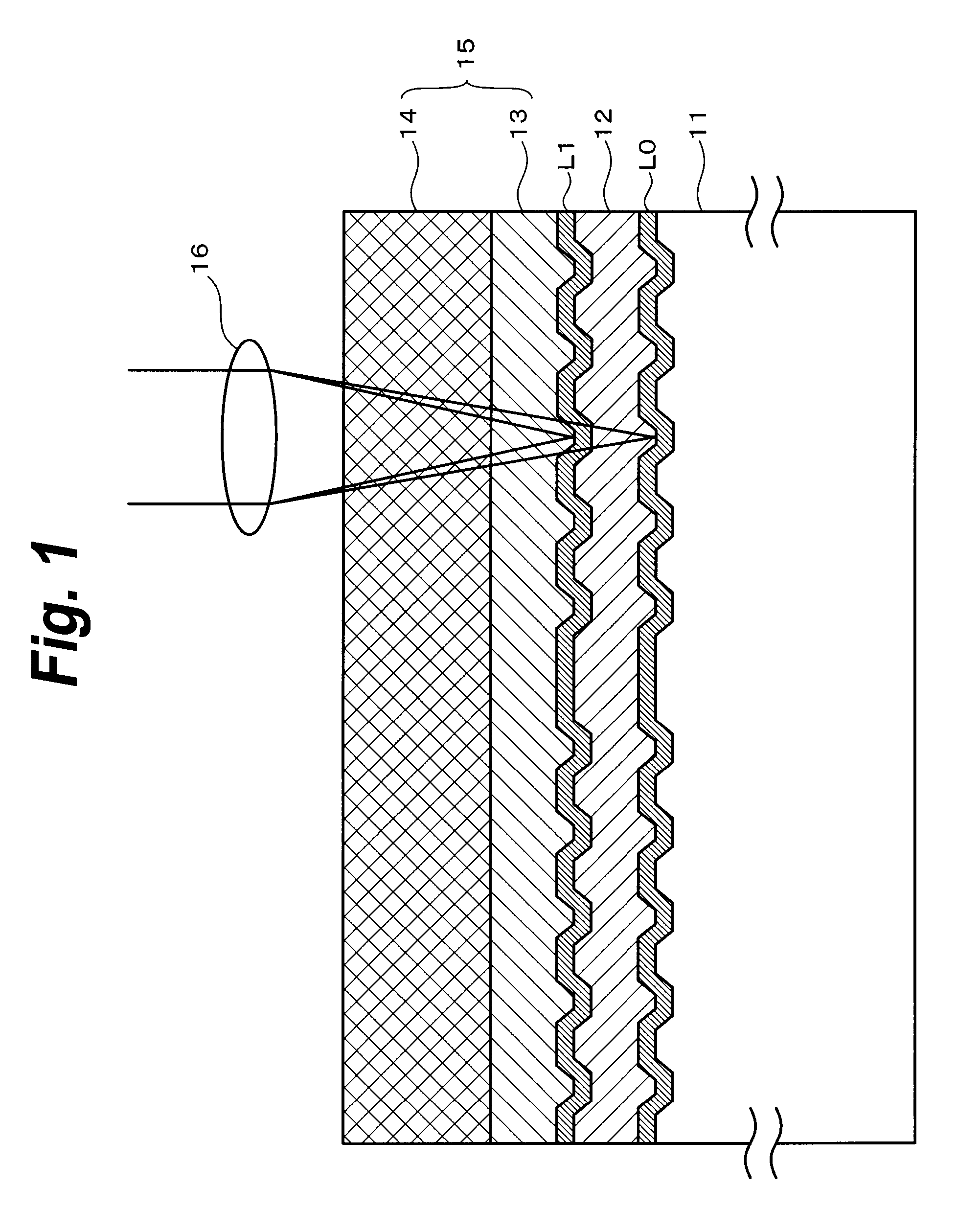
[0062] An embodiment of the invention will be described hereinbelow with reference to the drawings. An example of a high-density optical disk to which a manufacturing method according to an embodiment of the invention can be applied will be described with reference to FIG. 1.

[0063] In such an optical disk, an information signal is recorded and reproduced by irradiating a laser beam to an information recording layer from the side of a cover layer 15. For example, the laser beam having a wavelength of 400 to 410 nm is converged by an objective lens 16 having a numerical aperture (NA) of 0.84 to 0.86 and irradiated to either the L0 layer or the L1 layer serving as an information recording layer from the cover layer 15 side, so that the information signal is recorded or reproduced.

[0064] Such a high-density optical disk has a construction in which the L0 layer, an intermediate layer 12, the L1 layer, and the cover layer 15 are sequentially laminated onto a substrate 11. The cover laye...


PUM

PropertyMeasurementUnit
diameteraaaaaaaaaa
depthaaaaaaaaaa
depthaaaaaaaaaa

Abstract

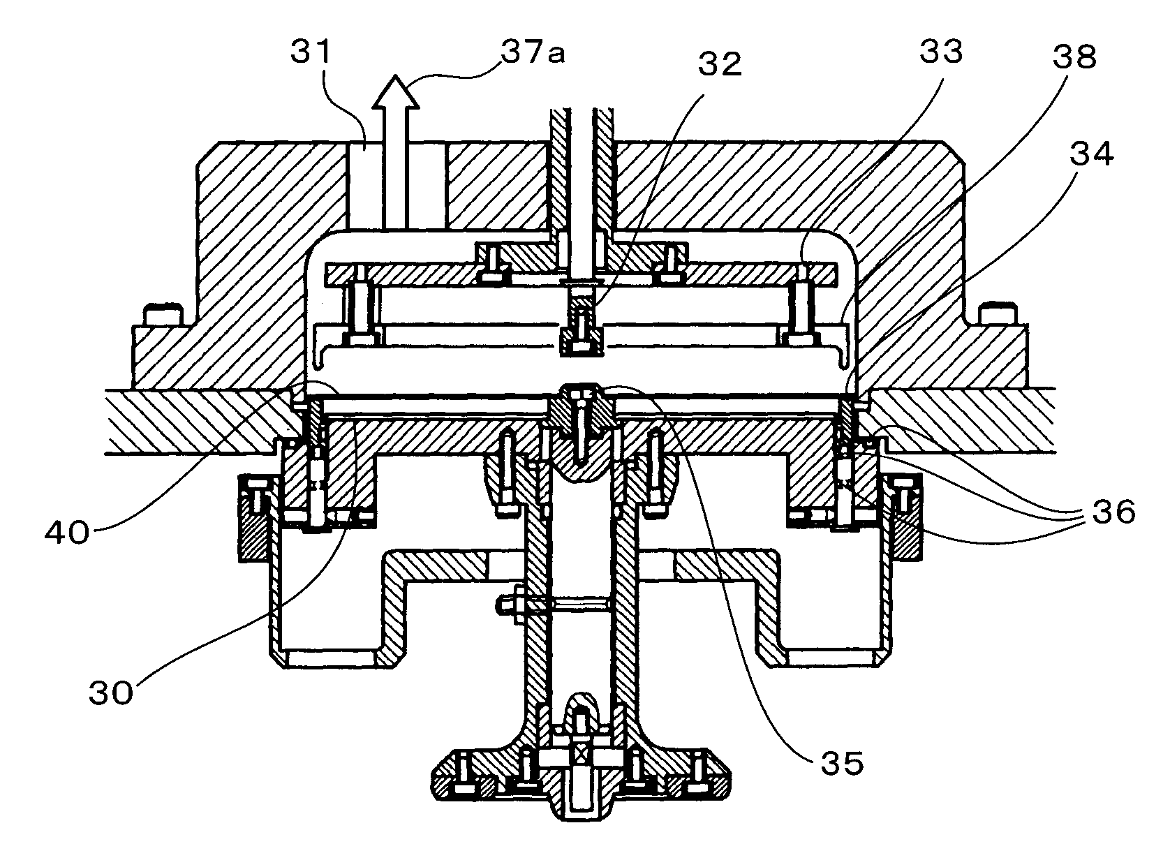
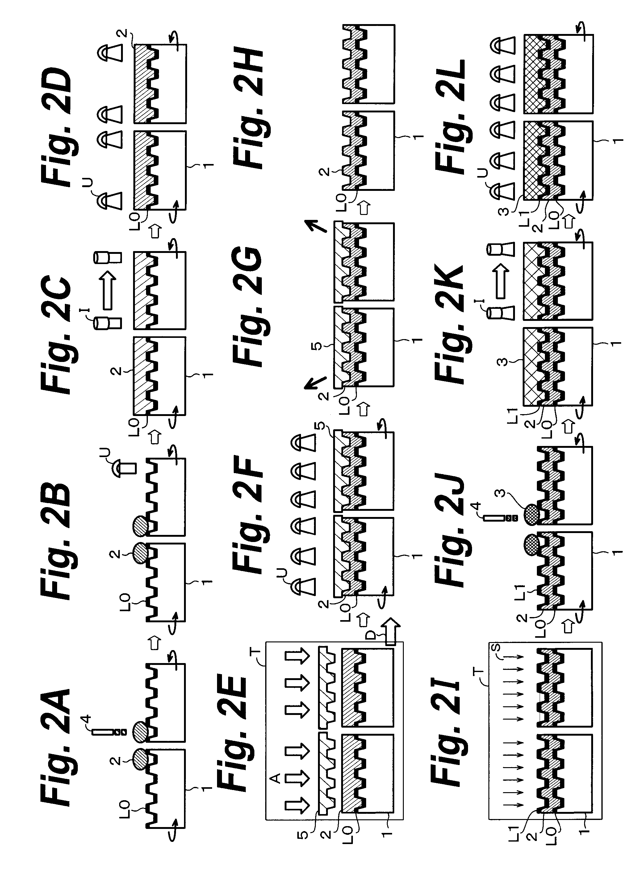
A manufacturing method of an optical disk in which information recording layers are formed onto a resin layer laminated on a substrate surface. The substrate surface is coated with the resin layer. The substrate and a stamper are arranged into a vacuum chamber so that the resin layer surface and the stamper surface with concave / convex portions face almost in parallel. The chamber is set into an almost vacuum state while holding the facing state of the substrate and the stamper. The chamber is changed from the almost vacuum state to an atmospheric pressure or higher. The substrate and the stamper are overlaid. The stamper is pressed by a differential pressure between the almost vacuum pressure and the atmospheric pressure or higher, thereby adhering the substrate and the stamper and transferring the concave / convex portions to the resin layer. The resin layer with the transferred concave / convex portions is hardened.

Description

CROSS REFERENCES TO RELATED APPLICATIONS [0001] The present invention contains subject matter related to Japanese Patent Application No.JP 2005-249379 filed on Aug. 30, 2006, and Japanese Patent Application No. JP 2006-143766 filed on May 24, 2006, the entire contents of which being incorporated herein by reference. BACKGROUND OF THE INVENTION [0002] 1. Field of the Invention [0003] The invention relates to a manufacturing method of an optical disk and its manufacturing apparatus and, more particularly, to a manufacturing method of an optical disk and its manufacturing apparatus which are applied to, for example, a multilayer optical disk having two or more information recording layers. [0004] 2. Description of the Related Arts [0005] In recent years, in the optical disk field, the realization of a large recording capacity is demanded. To realize the large recording capacity, it is considered that multilayer optical disks each having a plurality of information recording layers are d...

Claims


Application Information

Patent Timeline
Patent Type & Authority Applications(United States)
IPC IPC(8): B05D5/06B05D3/12C08F2/46B05C11/02C23C14/00
CPCB29C43/021B29C43/36B29C43/56B29C2043/025B29C2043/043B29C2043/3488G11B7/263B29C2043/3634B29C2043/561B29C2043/566B29C2791/006B29K2105/0002B29L2017/005B29C2043/3602Y02P20/582
Inventor WATANABE, HIDETOSHIAKIYAMA, SHOJI
Owner SONY CORP
Learn More