
Semiconductor heterostructure and method for forming same

a semiconductor heterostructure and heterostructure technology, applied in the direction of semiconductor/solid-state device manufacturing, semiconductor devices, electrical apparatus, etc., can solve the problems of not completely accepting the achieved surface properties of the semiconductor heterostructure when applying the above described prior art processes, rough surface is detrimental to the electrical behavior of the formed devices, and the surface roughness of the semiconductor heterostructure is not completely acceptable for further use. , to achieve the effect of reducing the surface roughness of the semiconductor heterostructure, improving the buried interfa

Active Publication Date: 2007-03-08
S O I TEC SILICON ON INSULATOR THECHNOLOGIES
View PDF14 Cites 24 Cited by
  • Summary
  • Abstract
  • Description
  • Claims
  • Application Information

AI Technical Summary

Benefits of technology

[0008] The invention now provide a method for forming a heterostructure and a corresponding semiconductor heterostructure which has significantly better surface roughness properties and / or significantly better buried interface roughness properties than the prior art. In particular, these advantages are achieved in a method for forming a semiconductor heterostructure that includes a substrate, a buffer layer and a top layer, wherein the method reduces surface roughness of the semiconductor heterostructure by providing the substrate with at least a surface layer having a first in-plane lattice parameter; providing the buffer layer with a second in-plane lattice parameter and providing the buffer layer upon the surface layer of the substrate; and providing an additional layer in between the buffer layer and the top layer, with the additional layer having a third in-plane lattice parameter which has a value in between those of the first and second lattice parameters.

Problems solved by technology

The structure obtained usually has a surface morphology that is not suitable for further use.
It appears, however, that the achieved surface properties for the semiconductor heterostructures are not completely acceptable when applying the above described prior art processes.
As the thickness of the strained silicon layer cannot exceed the critical thickness, beyond which defects would nucleate within the layer or at the interface of the strained and the underlying layers, this roughness can lead to defects.
A rough surface is also detrimental for the electrical behavior of the formed devices.

Method used


Image

  • Semiconductor heterostructure and method for forming same
  • Semiconductor heterostructure and method for forming same
  • Semiconductor heterostructure and method for forming same

Examples


first embodiment

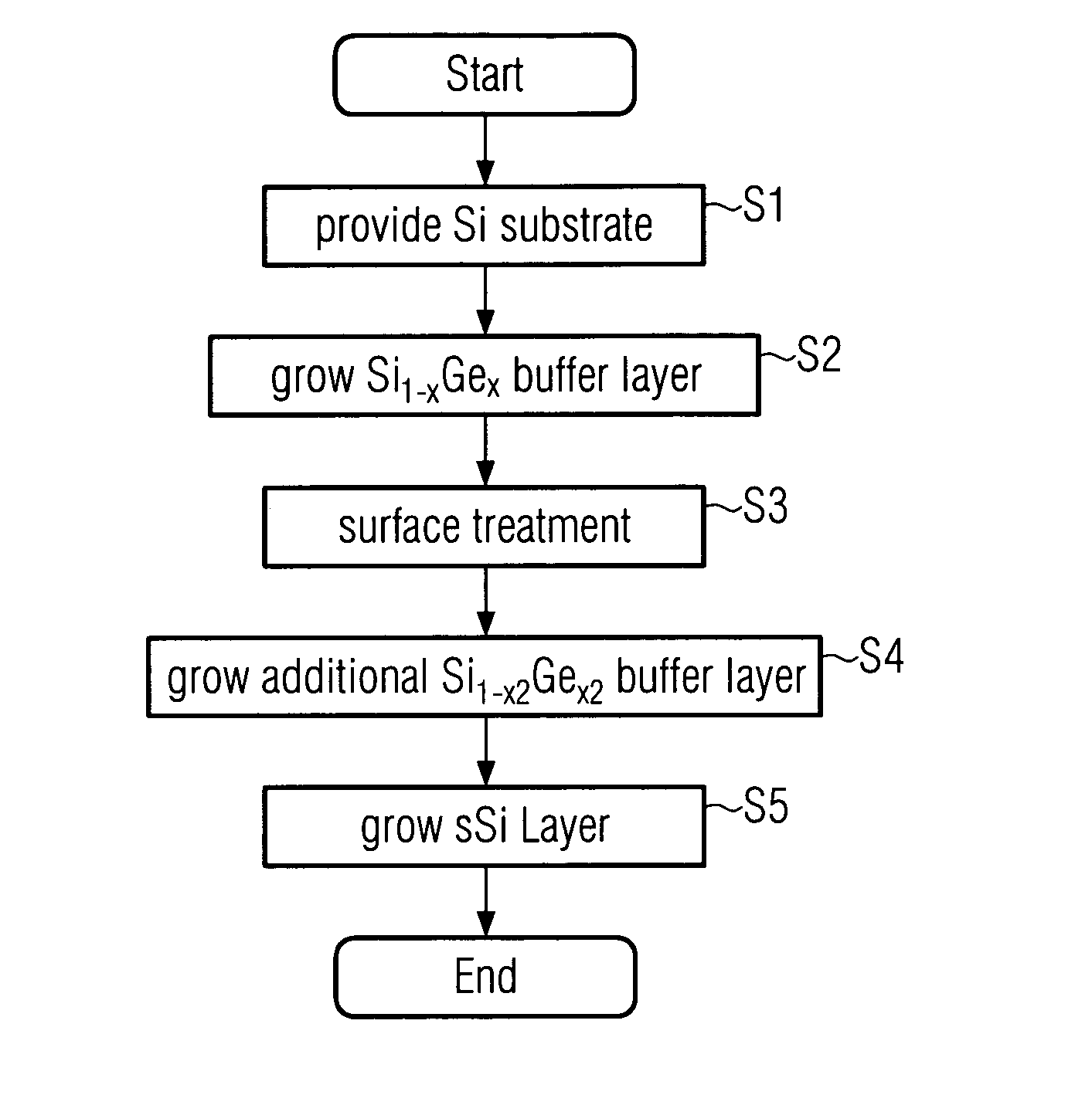
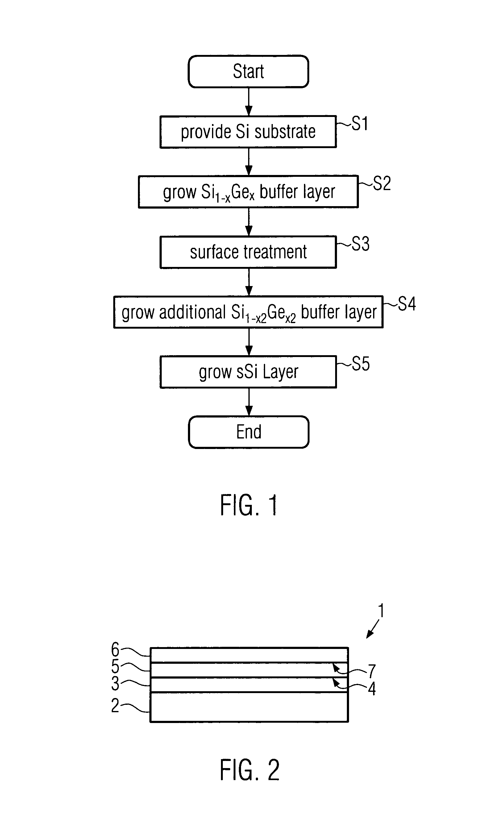
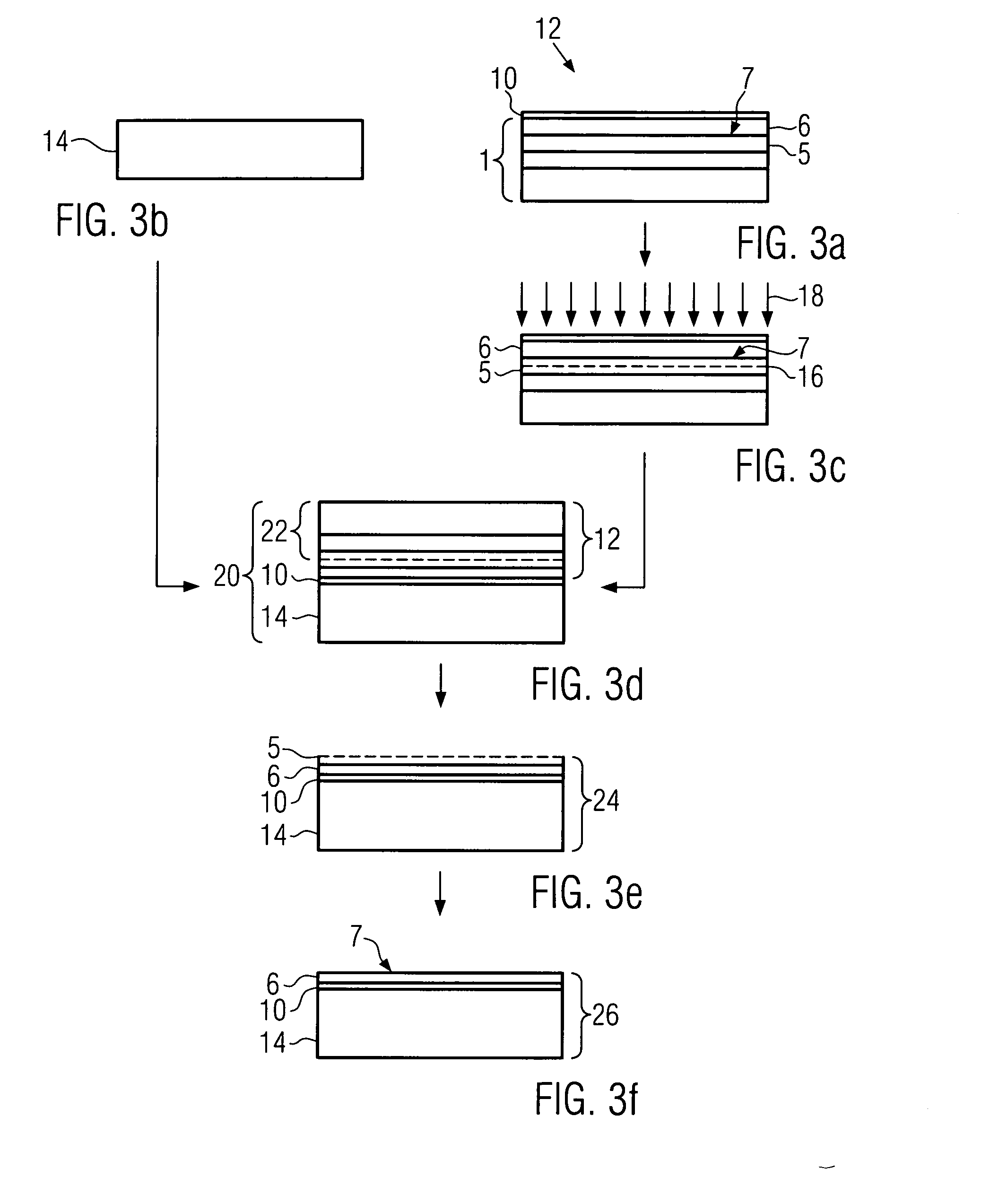
[0037]FIG. 1 is a block diagram illustrating the inventive method for forming a semiconductor heterostructure. In step S1 a silicon substrate is provided. Silicon substrates are readily available with different sizes and different crystalline surfaces. Then in step S2 a buffer layer of Si1-xGex is grown, preferably epitaxially, on the silicon substrate. The buffer layer can be a graded buffer layer, thus the concentration of the two compounds: silicon and germanium changes over the thickness of the buffer layer. By doing so the lattice parameter in the graded buffer slowly changes. For example, one can start with x=0 at the interface towards the silicon substrate, so that the lattice parameter corresponds to the one of the underlying Si substrate. Then the germanium concentration can grow until approximately 20%, thereby the in-plane lattice parameter becomes larger. It should be noted, however, that the final germanium concentration can be freely chosen, for instance 30% or 40%, an...


PUM


Abstract

The invention relates to a method for forming a semiconductor heterostructure by providing a substrate with a first in-plane lattice parameter a1, providing a buffer layer with a second in-plane lattice parameter a2 and providing a top layer over the buffer layer. In order to improve the surface roughness of the semiconductor heterostructure, an additional layer is provided in between the buffer layer and the top layer, wherein the additional layer has a third in-plane lattice parameter a3 which is in between the first and second lattice parameters.

Description

BACKGROUND ART [0001] The invention relates to a method for forming a semiconductor heterostructure comprising providing a substrate with a first in-plane lattice parameter a1, providing a buffer layer with a second in-plane lattice parameter a2, and providing a top layer over the buffer layer. The invention furthermore relates to the corresponding semiconductor heterostructure and to a semiconductor device that includes such semiconductor heterostructure. Semiconductor heterostructures like this are known from U.S. Pat. No. 5,442,205, which discloses semiconductor heterostructure devices with strained semiconductor layers. The known heterostructure includes a strained epitaxial layer of silicon or germanium which is located over a silicon substrate with a spatially graded GexSi1-x epitaxial layer, which in turn is overlaid by an ungraded capping layer Gex0Si1-x0, intervening between the silicon substrate and the strained layer. The graded layer and the capping layer therein play th...

Claims


Application Information

Patent Timeline
Patent Type & Authority Applications(United States)
IPC IPC(8): H01L29/732H01L33/00H01L33/12H01L33/34
CPCH01L21/02381H01L21/0245H01L21/02494H01L21/02502H01L21/76254H01L21/02524H01L21/02532H01L21/02587H01L21/0262H01L21/0251H01L29/161H01L29/205H01L29/225
Inventor FIGUET, CHRISTOPHEKENNARD, MARK
Owner S O I TEC SILICON ON INSULATOR THECHNOLOGIES
Learn More