Display device

a display device and display technology, applied in the field of display devices, can solve the problems of image quality deterioration, insufficient mobility of pixels, and failure to obtain desired display characteristics, and achieve the effect of simple circuit configuration

Inactive Publication Date: 2007-03-08
MITSUBISHI ELECTRIC CORP
View PDF9 Cites 41 Cited by
  • Summary
  • Abstract
  • Description
  • Claims
  • Application Information

AI Technical Summary

Benefits of technology

[0015] An object of the present invention is to provide a display device with a simple circuit configuration that enables a pixel TFT to be driven at

Problems solved by technology

In a wide operating temperature range, characteristic variations due to the temperatures of the respective parts of a display device may cause the problem of image quality deterioration.
Especially in a low temperature region, in some cases, a TFT disposed at a pixel does not have enough mobility, failing to obtain a desired display characteristic.
Hence, the TFT has poor mobility at low temperatures.
This results in a significant reduction in contrast due to a deficiency of charging to the pixel.
It is however extremely difficult to absorb variations (individual variations)

Method used


Image

  • Display device
  • Display device
  • Display device

Examples


first preferred embodiment

[0035] A. Configuration

[0036] A-1. Overall Configuration

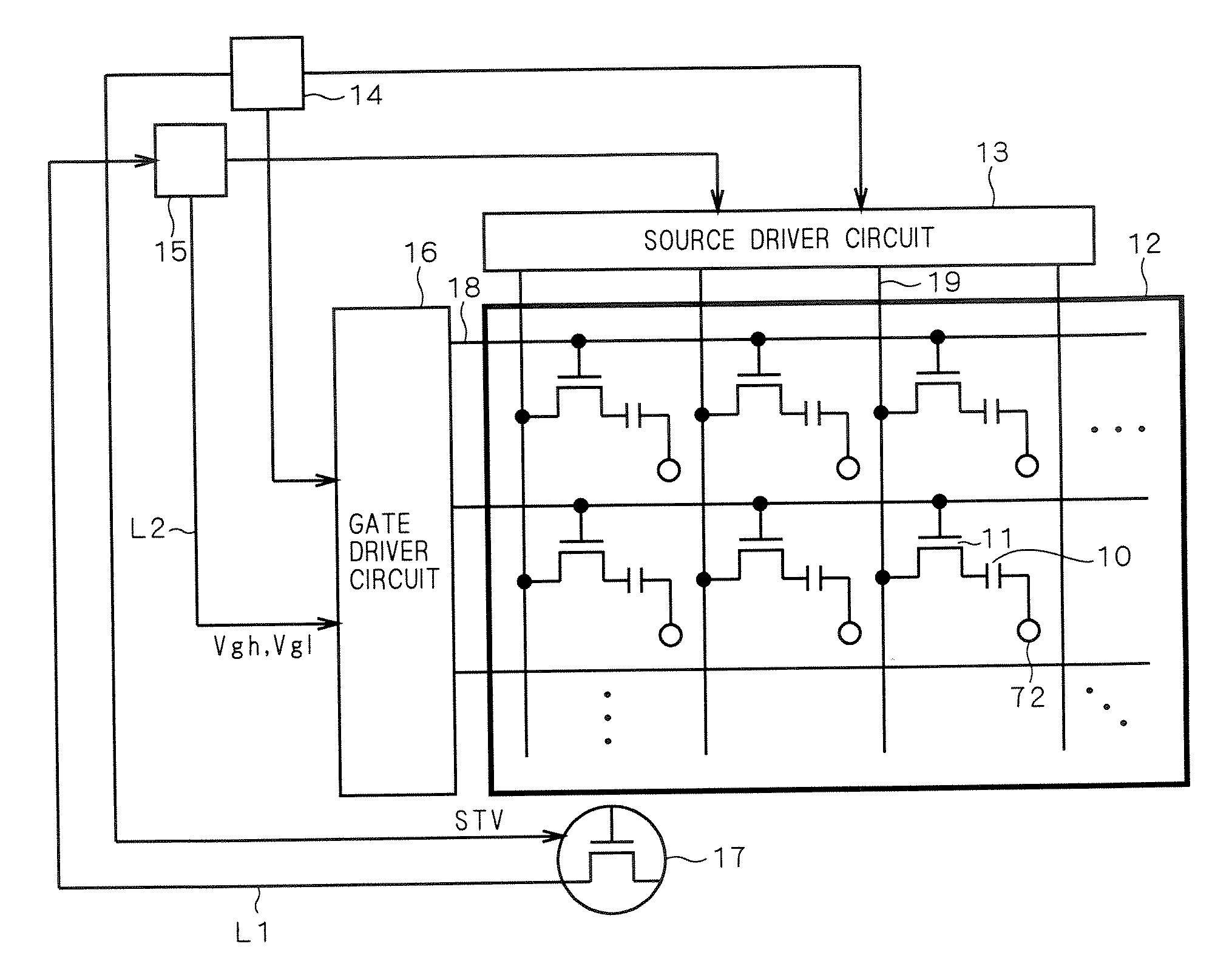
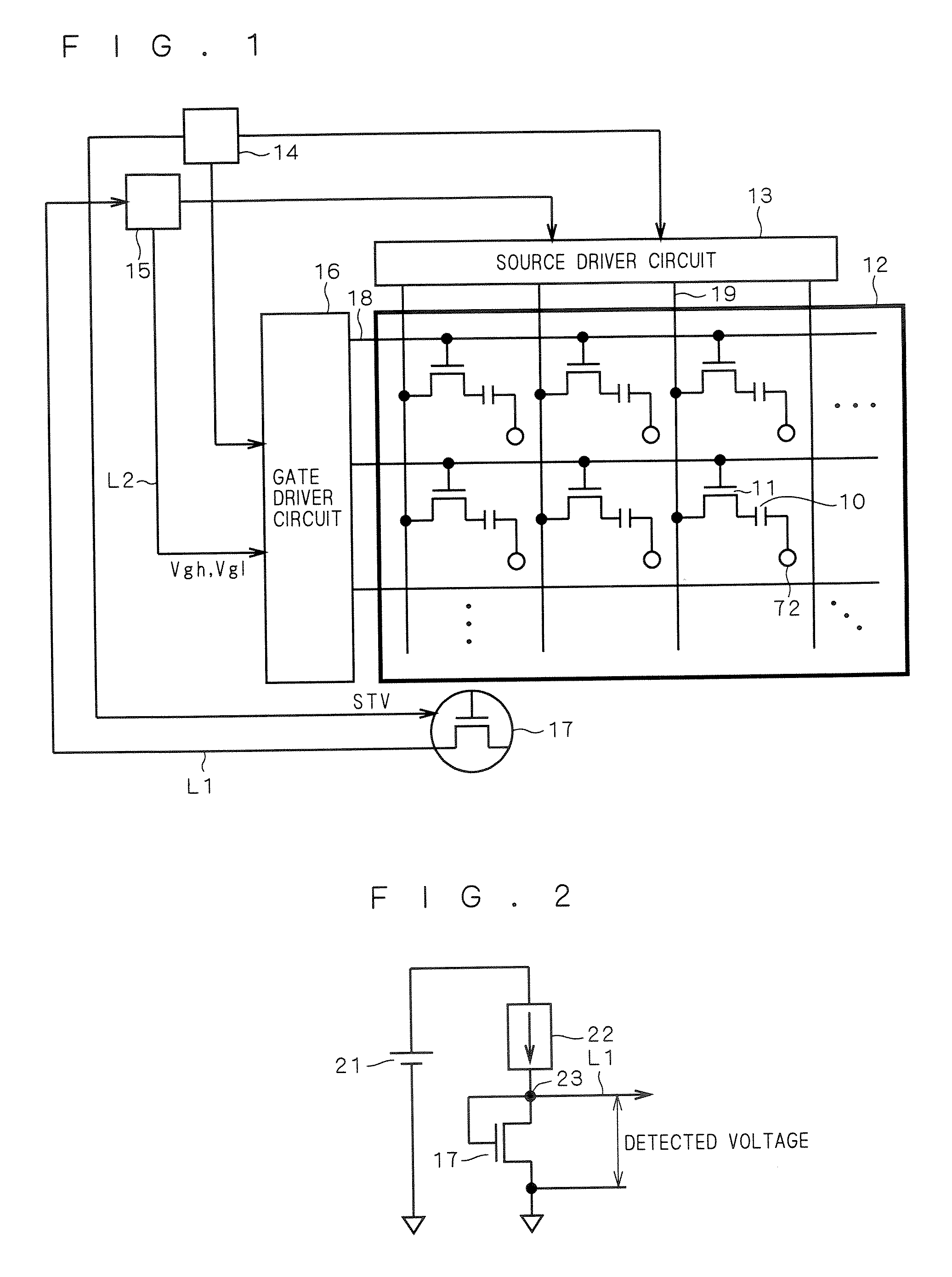
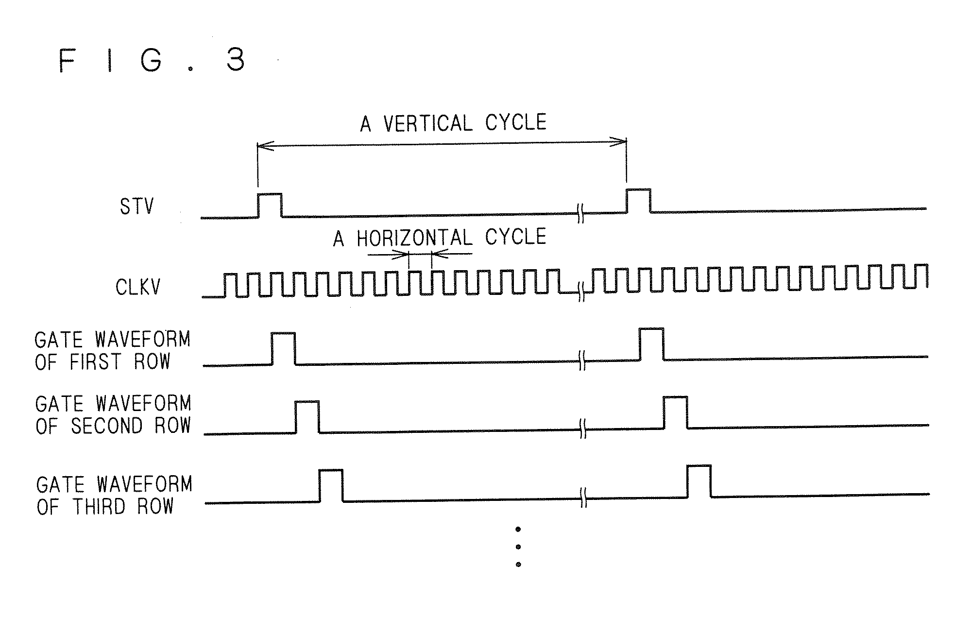
[0037]FIG. 1 is a block diagram of a display device according to a first preferred embodiment of the present invention. Pixels are arranged in a matrix-shape in a display area (a display region) 12 on a substrate, each of which is provided with a pixel TFT 11 that is an n-channel MOSFET.

[0038] A pixel capacity 10 is connected to the drain of each of the pixel TFTs 11. A gate driver circuit (a gate driving circuit) 16, which drives the pixel TFTs 11 per scanning line (gate wiring) 18, is connected to the gate of each of the pixel TFTs 11. A source driver circuit 13, which determines an applied voltage to the pixel capacity 10, is connected via a data line 19 to the source of each of the pixel TFTs 11.

[0039] One end of the pixel capacity 10 is connected to the drain of the pixel TFT 1, and the other end of the pixel capacity 10 is connected to a terminal 72. A later-described common voltage is applied to the terminal 72.

[004...

second preferred embodiment

[0131] In the display device of the first preferred embodiment, the description has been made of the case where the bias current generated at the constant current source 22 is flown to the TFT 17 for detecting characteristic in order to obtain the gate on voltage Vgh at that time.

[0132] In the display device of a second preferred embodiment, a gate driver circuit 16 drives a TFT 17 for detecting characteristic in order to detect the drain current Id passing through the TFT 17. By a feedback loop, the value of the gate on voltage Vgh is changed to obtain such a gate on voltage Vgh as to attain the drain current Id of a desired value (the value of the drain current Id required to charge the capacity Cp).

[0133] The configuration of the display device of the second preferred embodiment will be described below.

[0134] A. Configuration

[0135] A-1. Overall Configuration

[0136]FIG. 9 is a block diagram of the display device of the second preferred embodiment. The second preferred embodime...

third preferred embodiment

[0166] The first and second preferred embodiments have described the means for dynamically correcting the gate on voltage Vgh with the TFT 17 for detecting characteristic (refer to FIG. 1).

[0167] For example, in an LCD, the pixel TFTs 11 may deteriorate to cause a threshold shift and the like. Due to lack of the gate off voltage Vgl, the leak current may be increased to thereby deteriorate display quality.

[0168] For this reason, a display device according to a third preferred embodiment provides means for dynamically correcting a gate off voltage Vgl with the TFT 17 for detecting characteristic.

[0169] A. Configuration

[0170]FIG. 11 is a circuit diagram showing the configuration of peripheral circuits of a TFT 17 for detecting characteristic according to the third preferred embodiment.

[0171] A power source 112 is connected to the negative input terminal of an operational amplifier OP111 (a gate voltage control circuit). The power source 112 applies a reference voltage Vr to the n...


PUM


Abstract

There is disposed a TFT for detecting characteristic having the same characteristic as a pixel TFT disposed at a pixel. The TFT for detecting characteristic detects a gate on voltage for driving the pixel TFT. The TFT for detecting characteristic is driven so as to agree with the pixel TFT in a period of the on state. This provides a display device that is capable of driving the pixel TFT at its optimum driving voltage with a simple circuit configuration, even when the characteristic of the pixel TFT is subjected to temperature change, aged change, and individual variations.

Description

BACKGROUND OF THE INVENTION [0001] 1. Field of the Invention [0002] The present invention relates to a display device using a thin film transistor. [0003] 2. Description of the Background Art [0004] An active matrix display using a thin film transistor (TFT) as a switching element has been used for a variety of applications as a thin display device, such as one using a liquid crystal for optical control, and one using organic EL as a luminescent source. [0005] Examples of its typical applications are display devices of PCs, car navigation systems, ATMs, and POSs. Among these, the car navigation systems and the ATMs placed outdoors will be used under temperature environments in a very wide range, and the display devices are also required to operate in a wide temperature range. [0006] In a wide operating temperature range, characteristic variations due to the temperatures of the respective parts of a display device may cause the problem of image quality deterioration. Especially in a ...

Claims


Application Information

Patent Timeline
IPC IPC(8): G09G3/36
CPCG09G3/3208G09G3/3648G09G3/3655G09G2330/02G09G3/3696G09G2320/029G09G2320/041G09G3/3677G02F1/133
Inventor ISHIGUCHI, KAZUHIRO
Owner MITSUBISHI ELECTRIC CORP
Why Eureka
Try Eureka