Method of forming a phase changeable material layer, a method of manufacturing a phase changeable memory unit, and a method of manufacturing a phase changeable semiconductor memory device

a semiconductor memory and phase changeable technology, applied in the direction of solid-state devices, coatings, chemical vapor deposition coatings, etc., can solve the problems of difficult to precisely control the composition ratio, the electrical characteristics of the phase changeable material layer deteriorate, and the growth rate of the phase changeable material layer

Active Publication Date: 2007-03-08
SAMSUNG ELECTRONICS CO LTD
View PDF5 Cites 63 Cited by
  • Summary
  • Abstract
  • Description
  • Claims
  • Application Information

AI Technical Summary

Benefits of technology

[0023] The foregoing and/or other aspects of the present invention are also achieved by providing a phase changeable memory device, including at least one memory unit. The at least one memory unit includes a substrate having a plurality of terminal regions including one or more source regions, one or more drain regions, and one or more gate structures, one or more lower electrode contact structures arranged in electrical contact with o

Problems solved by technology

However, when using the conventional PVD process, it is difficult to control a growth rate of the phase changeable material layer.
When forming the phase changeable material layer using the PVD process, the electrical characteristics of the phase changeable materi

Method used


Image

  • Method of forming a phase changeable material layer, a method of manufacturing a phase changeable memory unit, and a method of manufacturing a phase changeable semiconductor memory device
  • Method of forming a phase changeable material layer, a method of manufacturing a phase changeable memory unit, and a method of manufacturing a phase changeable semiconductor memory device
  • Method of forming a phase changeable material layer, a method of manufacturing a phase changeable memory unit, and a method of manufacturing a phase changeable semiconductor memory device

Examples


example 1

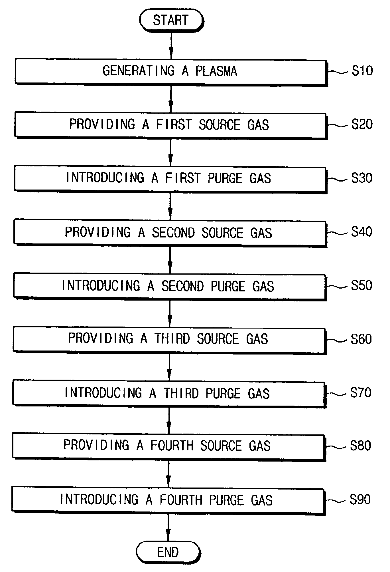
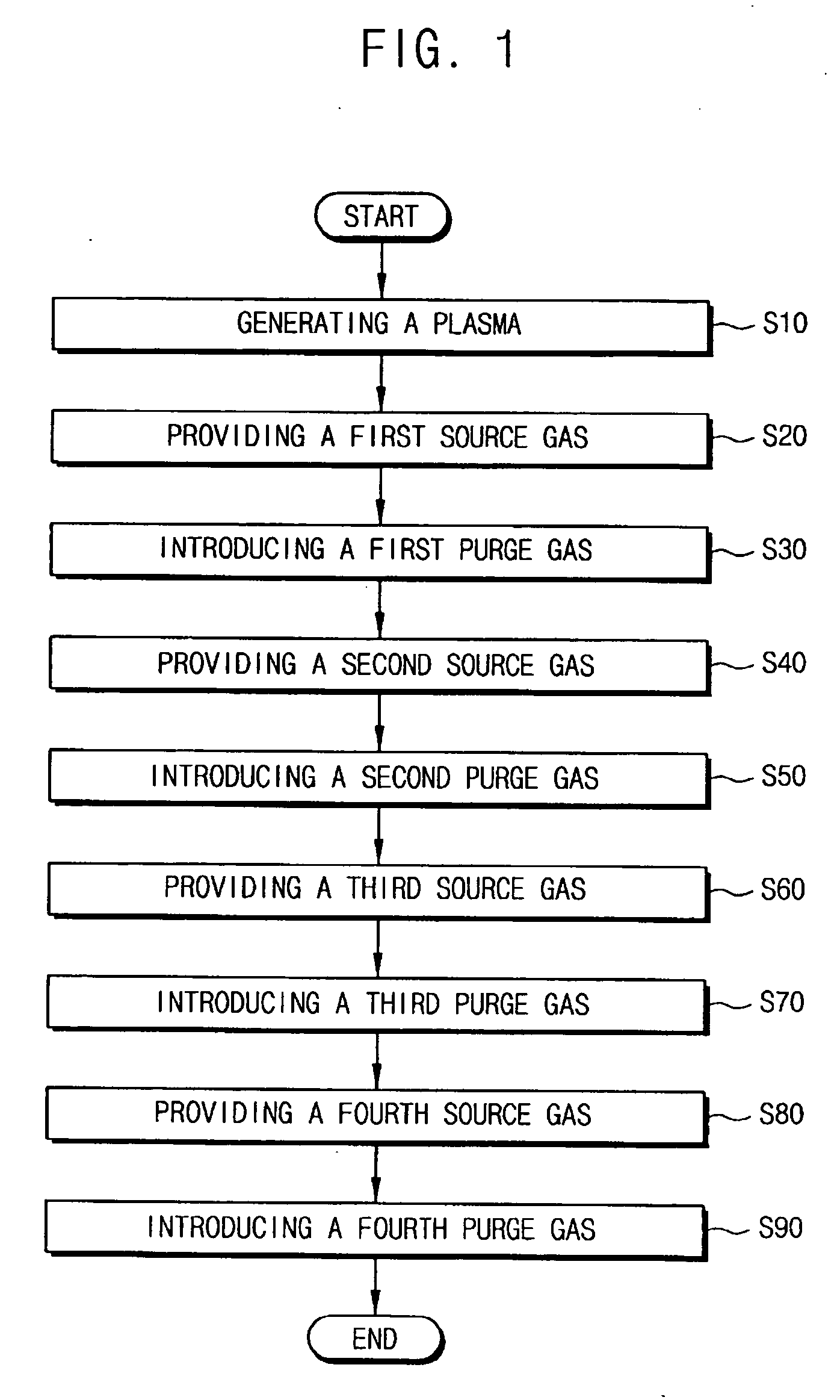
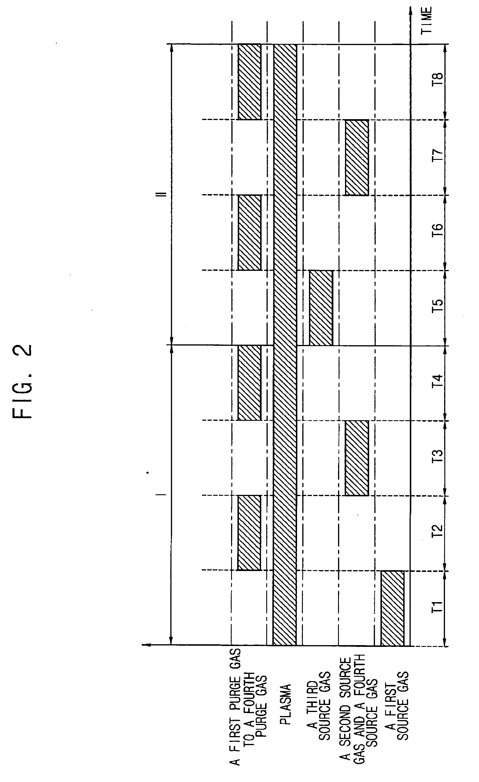
[0121] After providing a first source gas including germanium on a substrate for about 1.0 second, a first composite material layer was formed on the substrate by providing a second source gas including tellurium on the substrate for about 0.2 seconds. A third source gas including antimony was provided on the first composite material layer for about 0.4 seconds, and then a second composite material layer was formed on the substrate by providing a fourth source gas including tellurium on the first composite material layer for about 0.2 seconds. Thus, a phase changeable material layer including germanium, antimony and tellurium was formed on the substrate. A concentration ratio of germanium, antimony and tellurium in the phase changeable material layer was about 33.3:13.037:52.7, respectively.

example 2

[0122] After providing a first source gas including germanium on a substrate for about 1.0 second, a first composite material layer was formed on the substrate by providing a second source gas including tellurium on the substrate for about 0.3 seconds. A third source gas including antimony was provided on the first composite material layer for about 0.4 seconds, and then a second composite material layer was formed on the substrate by providing a fourth source gas including tellurium on the first composite material layer for about 0.2 seconds. Thus, a phase changeable material layer including germanium, antimony, and tellurium was formed on the substrate. A concentration ratio of germanium, antimony, and tellurium in the phase changeable material layer was about 26.9:15.1:56.3, respectively.

example 3

[0123] After providing a first source gas including germanium on a substrate for about 1.0 second, a first composite material layer was formed on the substrate by providing a second source gas including tellurium on the substrate for about 0.4 seconds. A third source gas including antimony was provided on the first composite material layer for about 0.4 seconds, and then a second composite material layer was formed on the substrate by providing a fourth source gas including tellurium on the first composite material layer for about 0.4 seconds. Thus, a phase changeable material layer including germanium, antimony and tellurium was formed on the substrate. A concentration ratio of germanium, antimony and tellurium in the phase changeable material layer was about 21.59:14.5:61.9, respectively.


PUM

PropertyMeasurementUnit
Temperatureaaaaaaaaaa
Timeaaaaaaaaaa

Abstract

A phase changeable material layer usable in a semiconductor memory device and a method of forming the same are disclosed. The method includes forming a plasma in a chamber having a substrate disposed therein, providing a first source gas including a germanium based material to form a first layer including the germanium based material on the substrate while maintaining the plasma in the chamber, providing a second source gas including a tellurium based material to react with the first layer to form a first composite material layer including a germanium-tellurium composite material on the substrate while maintaining the plasma in the chamber, providing a third source gas including an antimony based material to form a second layer including the antimony based material on the first composite material layer while maintaining the plasma in the chamber, and providing a fourth source gas including tellurium based material to react with the second layer including antimony based material to form a second composite material layer including an antimony-tellurium composite material on the first composite material layer. Accordingly, the phase changeable material layer may be formed at a low temperature and power to have desirable electrical characteristics.

Description

CROSS-REFERENCE TO RELATED APPLICATIONS [0001] This application claims the benefit under 35 U.S.C. §119(a) of Korean Patent Application No. 2005-81965, filed Sep. 3, 2005 in the Korean Intellectual Property Office, the entire contents of which are incorporated herein by reference BACKGROUND OF THE INVENTION [0002] 1. Field of the Invention [0003] Example embodiments of the present invention relate to a method of forming a phase changeable material layer, a method of manufacturing a phase changeable memory unit, and a phase changeable semiconductor memory device using the same. More particularly, example embodiments of the present invention relates a method of forming a phase changeable material layer including chalcogenide, a method of manufacturing a phase changeable memory unit using the same, and a phase changeable semiconductor memory device using the same. [0004] 2. Description of the Related Art [0005] A phase changeable memory device stores information using structural phase ...

Claims


Application Information

Patent Timeline
IPC IPC(8): H01L21/20H01L21/36H01L31/20
CPCC23C16/305H01L27/2436H01L45/06H01L45/1683H01L45/144H01L45/1616H01L45/1675H01L45/1233H10B63/30H10N70/231H10N70/023H10N70/8828H10N70/826H10N70/063H10N70/066
Inventor LEE, JIN-ILLEE, CHOONG-MANCHO, SUNG-LAEPARK, YOUNG-LIM
Owner SAMSUNG ELECTRONICS CO LTD
Why Eureka
Try Eureka