Semiconductor storage apparatus
a technology of semiconductors and storage devices, applied in the field of semiconductor storage devices, can solve problems such as complex hardware construction, and achieve the effect of simplifying hardware construction
- Summary
- Abstract
- Description
- Claims
- Application Information
AI Technical Summary
Benefits of technology
Problems solved by technology
Method used
Image

Examples
embodiment 1
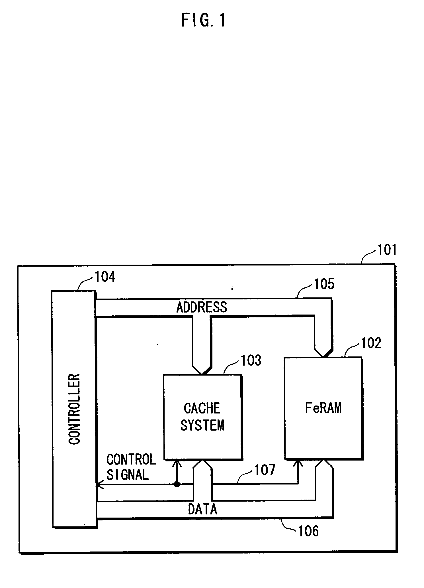
[0044]FIG. 1 shows an outline construction of a semiconductor storage apparatus in Embodiment 1.
[0045] A semiconductor storage apparatus 101 includes a ferroelectric memory 102, a cache system 103, a controller 104, an address bus 105, a data bus 106, and a control bus 107. The ferroelectric memory 102, the cache system 103, and the controller 104 are inter-connected by the address bus 105, the data bus 106, and the control bus 107.
[0046] The ferroelectric memory 102 includes a plurality of unit storage areas in which data is stored. Upon receiving, via the control bus 107, a control signal representing a read request, the ferroelectric memory 102 outputs data which is stored in a unit storage area that is specified via the address bus 105, via the data bus 106. Also, upon receiving, via the control bus 107, a control signal representing a rewrite request, the ferroelectric memory 102 replaces the data stored in a unit storage area that is specified via the address bus 105, with t...
embodiment 2
[0123]FIG. 7 shows an outline construction of a semiconductor storage apparatus in Embodiment 2.
[0124] A semiconductor storage apparatus 201 includes a ferroelectric memory 202, a cache system 203, a flash controller 204, address buses 205a and 205b, a data bus 206, a control bus 207, and a flash memory 208.
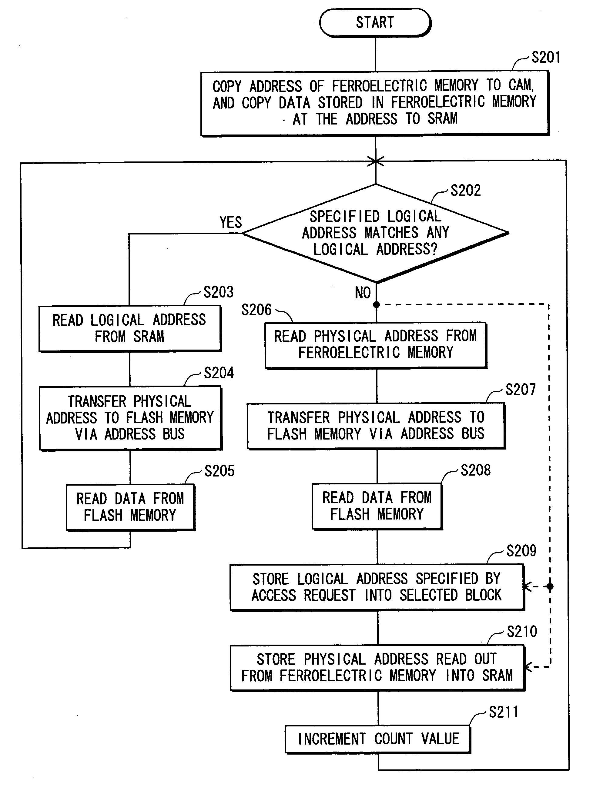
[0125] The semiconductor storage apparatus in Embodiment 2 uses the flash memory 208 as a storage medium for storing data, and uses the ferroelectric memory 202 as a storage medium for storing an address conversion table. The address conversion table shows correspondence between physical addresses and logical addresses of the flash memory 208.
[0126] In general, in the flash memory, data is rewritten in units of data blocks. When all data in a data block is rewritten, it simply requires that the data block is overwritten. However, when data in a data block is partially rewritten, the data is transferred from the block to another block, and the data is partially rewritten. Accor...
embodiment 3
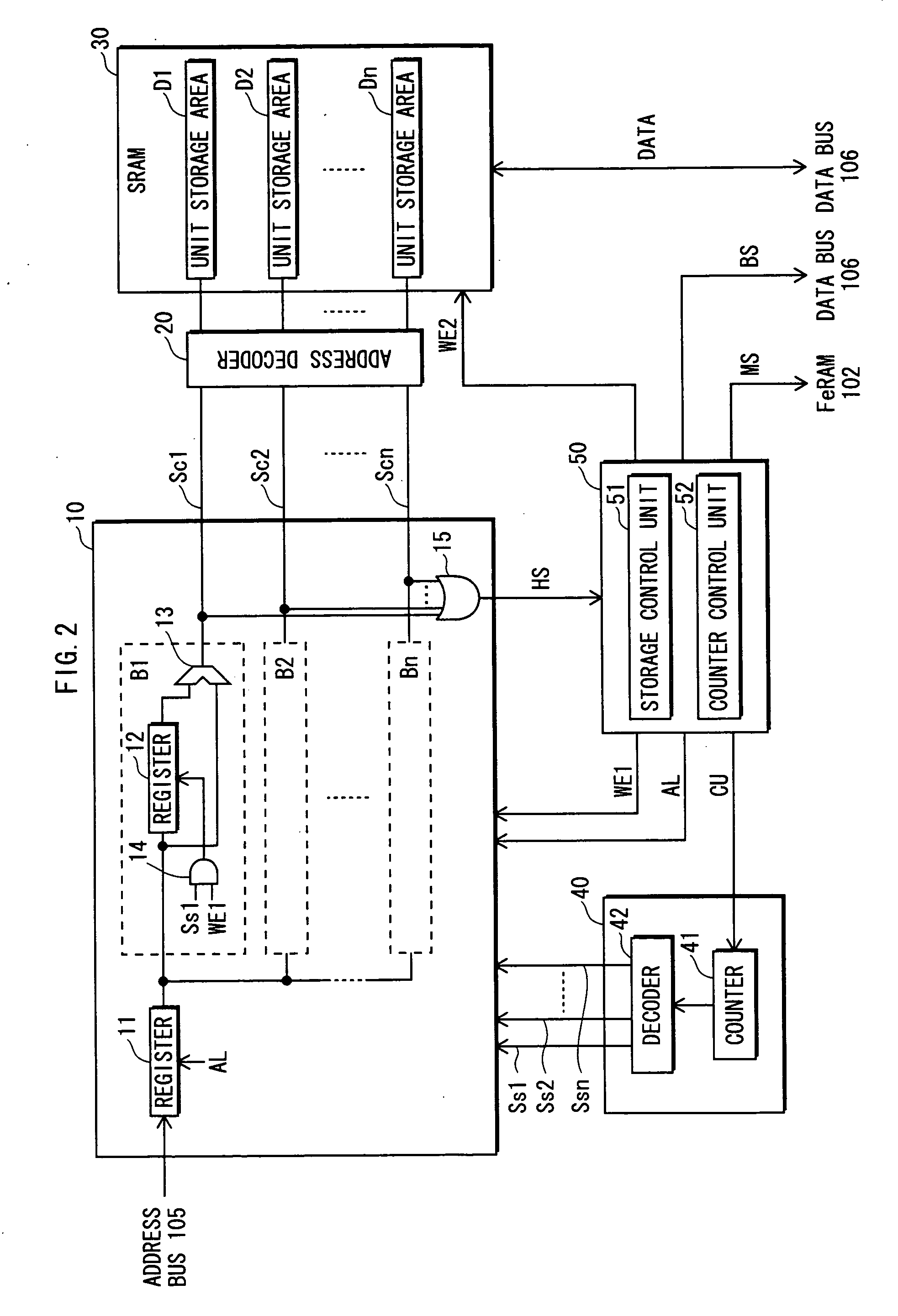
[0193]FIG. 13 shows the construction of the cache system 203 in Embodiment 3.
[0194] In Embodiment 3, the flash memory 208 is used as a storage medium in a semiconductor storage apparatus, as in Embodiment 2. Embodiment 3 differs from Embodiment 2 only by a control unit 60. The other constructions are the same as those of Embodiment 2, and the description thereof is omitted.
[0195] The control unit 60 receives a mode switch signal MSS from the flash controller 204. The mode switch signal MSS is used to indicate a normal mode (non-power-saving mode) or in a power-saving mode in which an operation is performed when a request to rewrite the physical address PBA is received and a cache mishit is detected. In the normal mode, both the cache system 203 and the ferroelectric memory 202 store the physical address PBA, which is the same operation as in Embodiment 2. On the other hand, in the power-saving mode, the cache system 203 does not store the physical address PBA, and only the ferroel...
PUM
 Abstract
Description
Claims
Application Information
 - Generate Ideas
- Intellectual Property
- Life Sciences
- Materials
- Tech Scout
- Unparalleled Data Quality
- Higher Quality Content
- 60% Fewer Hallucinations
Browse by: Latest US Patents, China's latest patents, Technical Efficacy Thesaurus, Application Domain, Technology Topic, Popular Technical Reports.
© 2025 PatSnap. All rights reserved.Legal|Privacy policy|Modern Slavery Act Transparency Statement|Sitemap|About US| Contact US: help@patsnap.com