Metal insulator semiconductor field effect transistor having fin structure

a technology of metal insulator and semiconductor field, applied in the direction of semiconductor devices, radio frequency controlled devices, electrical equipment, etc., can solve the problems of increased impurity concentration of channels, high off-leak current, and easy production of short-channel effects

Active Publication Date: 2007-03-22
MICROSOFT TECH LICENSING LLC
View PDF2 Cites 34 Cited by
  • Summary
  • Abstract
  • Description
  • Claims
  • Application Information

AI Technical Summary

Problems solved by technology

The Fin-FET therefore has the problem that off-leak currents are high (or short-channel effects are easy to produce).
However, the punch-through stopper layer increases the impurity concentration of the channel.
The increase in impurity concentration is likely to degrade the performance of the Fin-FET, e.g., to lower the mobility of electrons, to increase a source-to-drain junction leak (capacitance), and to vary in threshold value.

Method used


Image

  • Metal insulator semiconductor field effect transistor having fin structure
  • Metal insulator semiconductor field effect transistor having fin structure
  • Metal insulator semiconductor field effect transistor having fin structure

Examples


first embodiment

[0038] [First Embodiment]

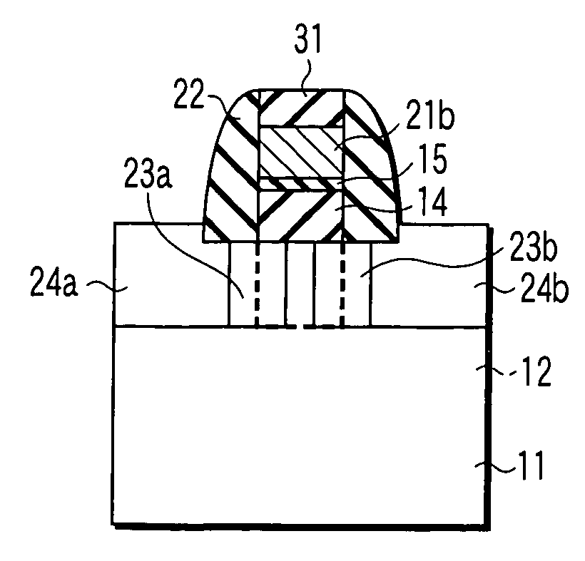
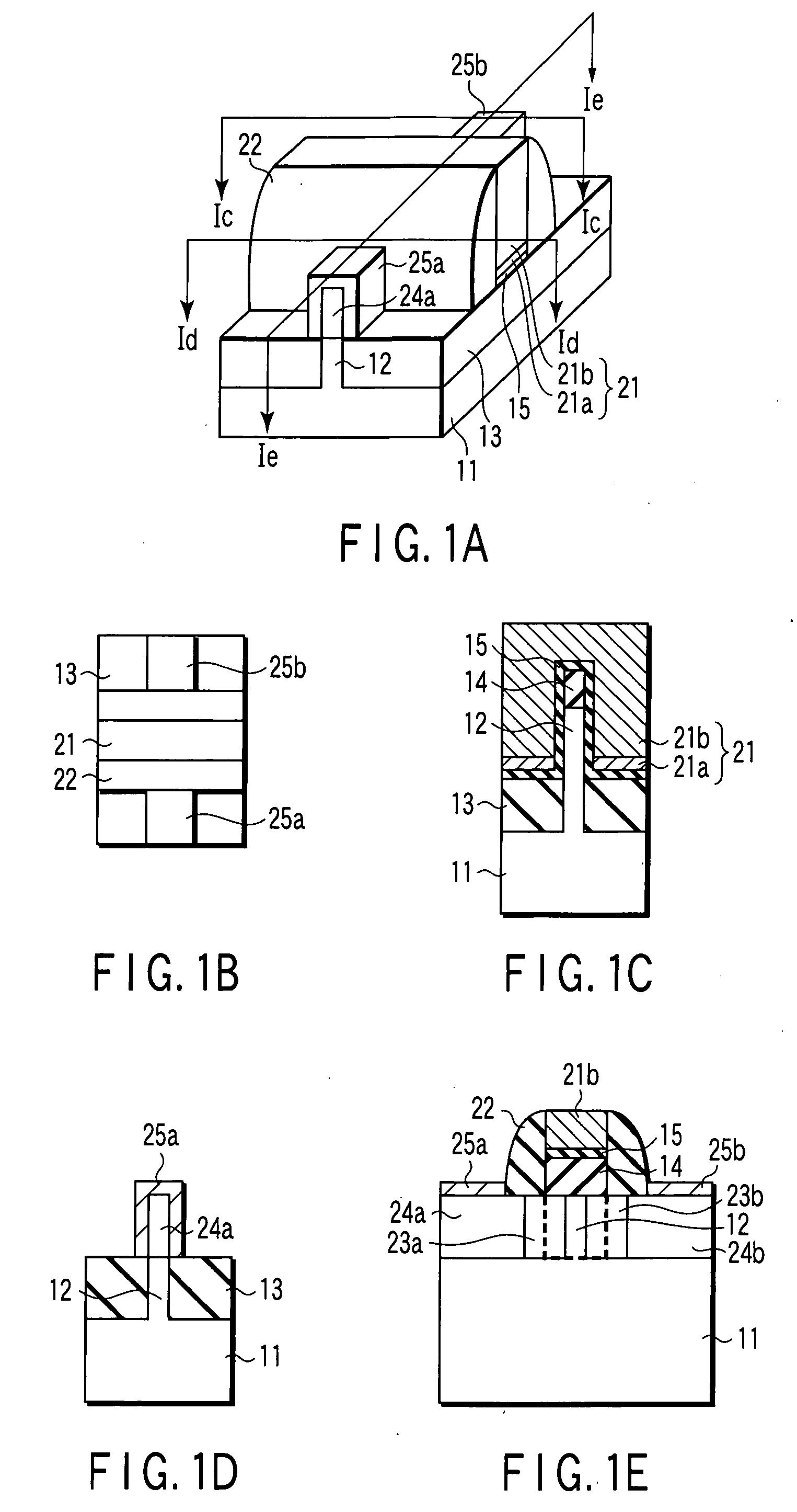
[0039]FIGS. 1A to 1E show a basic configuration of a semiconductor device (Fin-FET) according to a first embodiment of the present invention. Of these figures, FIG. 1A is a perspective view thereof, FIG. 1B is a plan view thereof, FIG. 1C is a sectional view taken along line Ic—Ic of FIG. 1A, FIG. 1D is a sectional view taken along line Id—Id of FIG. 1A, and FIG. 1E is a sectional view taken along line Ie—Ie of FIG. 1A. In the first embodiment, a fin is formed by processing part of a substrate into a desired shape, and a gate electrode section is formed of metal.

[0040] Referring to FIGS. 1A to 1E, a fin (fin-shaped semiconductor layer) 12, which is made of, e.g., single-crystal silicon, is formed on the surface of a silicon substrate (semiconductor substrate) 11. The fin 12 is provided in almost the middle of the top surface of the substrate 11 and along the lengthwise direction thereof, as shown in FIG. 1A. The fin 12 has a given width, a given height and ...

second embodiment

[0066] [Second Embodiment]

[0067]FIGS. 17A to 17E show a basic configuration of a semiconductor device (Fin-FET) according to a second embodiment of the present invention. Of these figures, FIG. 17A is a perspective view thereof, FIG. 17B is a plan view thereof, FIG. 17C is a sectional view taken along line XVIIc-XVIIc of FIG. 17A, FIG. 17D is a sectional view taken along line XVIId-XVIId of FIG. 17A, and FIG. 17E is a sectional view taken along line XVIIe-XVIIe of FIG. 17A. The same components as those of the Fin-FET according to the first embodiment (see FIGS. 1A to 1E) are denoted by the same reference numerals and their detailed descriptions are omitted.

[0068] As shown in FIGS. 17A to 17E, the Fin-FET according to the second embodiment differs from the Fin-FET according to the first embodiment in that a first gate electrode 21A-a of a gate electrode section 21A is provided to correspond to only part of a second gate electrode 21A-b that is adjacent to at least a fin 12.

[0069] A...

third embodiment

[0077] [Third Embodiment]

[0078]FIGS. 21A to 21E show a basic configuration of a semiconductor device (Fin-FET) according to a third embodiment of the present invention. Of these figures, FIG. 21A is a perspective view thereof, FIG. 21B is a plan view thereof, FIG. 21C is a sectional view taken along line XXIc-XXIc of FIG. 21A, FIG. 21D is a sectional view taken along line XXId-XXId of FIG. 21A, and FIG. 21E is a sectional view taken along line XXIe-XXIe of FIG. 21A. In the third embodiment, a fin is selectively formed on a substrate by selective epitaxial growth. The same components as those of the Fin-FET according to the first embodiment (see FIGS. 1A to 1E) are denoted by the same reference numerals and their detailed descriptions are omitted.

[0079] As shown in FIGS. 21A to 21E, the Fin-FET according to the third embodiment differs from the Fin-FET according to the first embodiment in that a fin 12B is selectively formed on the top surface of a silicon substrate 11B by selective...


PUM


Abstract

A semiconductor device includes a fin-shaped semiconductor layer, a gate electrode section formed in a widthwise direction of the semiconductor layer with a gate insulation film interposed therebetween, the gate electrode section including a plurality of electrode materials having different work functions and stacked one another, and a channel section formed adjacent to the gate insulation film in the semiconductor layer. The semiconductor device further includes source and drain regions formed adjacent to the channel section.

Description

CROSS-REFERENCE TO RELATED APPLICATIONS [0001] This application is based upon and claims the benefit of priority from prior Japanese Patent Application No. 2005-270772, filed Sep. 16, 2005, the entire contents of which are incorporated herein by reference. BACKGROUND OF THE INVENTION [0002] 1. Field of the Invention [0003] The present invention relates to a semiconductor device. More specifically, the invention relates to a metal insulator semiconductor field effect transistor (MISFET) having a fin-type structure. [0004] 2. Description of the Related Art [0005] A prior art fin-type MISFET (abbreviated as Fin-FET hereinafter) has a structure in which the source / drain easily causes a punch-through phenomenon on the bottom of a fin corresponding to the edge (bottom) of a gate electrode. The Fin-FET therefore has the problem that off-leak currents are high (or short-channel effects are easy to produce). See, for example, Masaki Kondo et al., “A FinFET Design Based on Three-Dimensional P...

Claims


Application Information

Patent Timeline
Patent Type & Authority Applications(United States)
IPC IPC(8): H01L27/10H01L29/73H01L29/768H01L27/148
CPCH01L21/823412H01L21/823437H01L29/7851H01L29/4908H01L29/66795H01L29/42384
Inventor WATANABE, TAKESHIOKANO, KIMITOSHIIZUMIDA, TAKASHI
Owner MICROSOFT TECH LICENSING LLC
Why Eureka
Try Eureka