Necked Finfet device

a technology of finfet and finfet, which is applied in the direction of semiconductor devices, electrical equipment, transistors, etc., can solve problems affecting device performance, and achieve the effects of reducing finfet channel resistance, preventing silicide formation, and improving device performan

Inactive Publication Date: 2007-03-22
TAIWAN SEMICON MFG CO LTD
View PDF14 Cites 34 Cited by
  • Summary
  • Abstract
  • Description
  • Claims
  • Application Information

AI Technical Summary

Benefits of technology

[0008] It is another object of this invention to reduce FINFET channel resistance via formation of a necked portion of channel region, only in a portion of a wider conductive region located between source and drain regions.
[0009] It is still another object of this invention to form a wrap up insulator spacer on the sides of the FINFET device to prevent silicide formation on exposed sides of the mesa like FINFET device.
[0010] In accordance with the present invention a method of fabricating a double gate FINFET device structure in a SOI layer, wherein features such as a necked channel region and a wrap up insulator spacer are employed to improve device performance, is described. Definition of the silicon layer component of the SOI layer, and of an overlying hard mask insulator layer, results in a raised structure comprised of a silicon source / drain shapes connected by a narrower channel region shape wherein a center portion of the raised silicon channel region shape is necked or narrowed. A thermal oxidation procedure results in the formation of a gate insulator layer on both sides of the necked channel region shape, followed by definition of a conductive gate structure formed normal in direction to the channel region shape, overlying the gate insulator layers located on both sides of the necked portion of the channel region shape. Removal of the hard mask insulator layer from portions of the silicon source / drain shapes is followed by formation of a source / drain region in the silicon source / drain shapes. A wrap up, composite insulator spacer is next formed on the sides of the raised silicon structure, protecting against a procedure used to form metal silicide on exposed portions of source / drain regions.

Problems solved by technology

This can result in unwanted channel resistance, adversely influencing device performance.

Method used


Image

  • Necked Finfet device
  • Necked Finfet device
  • Necked Finfet device

Examples


Embodiment Construction

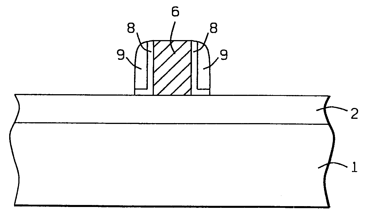
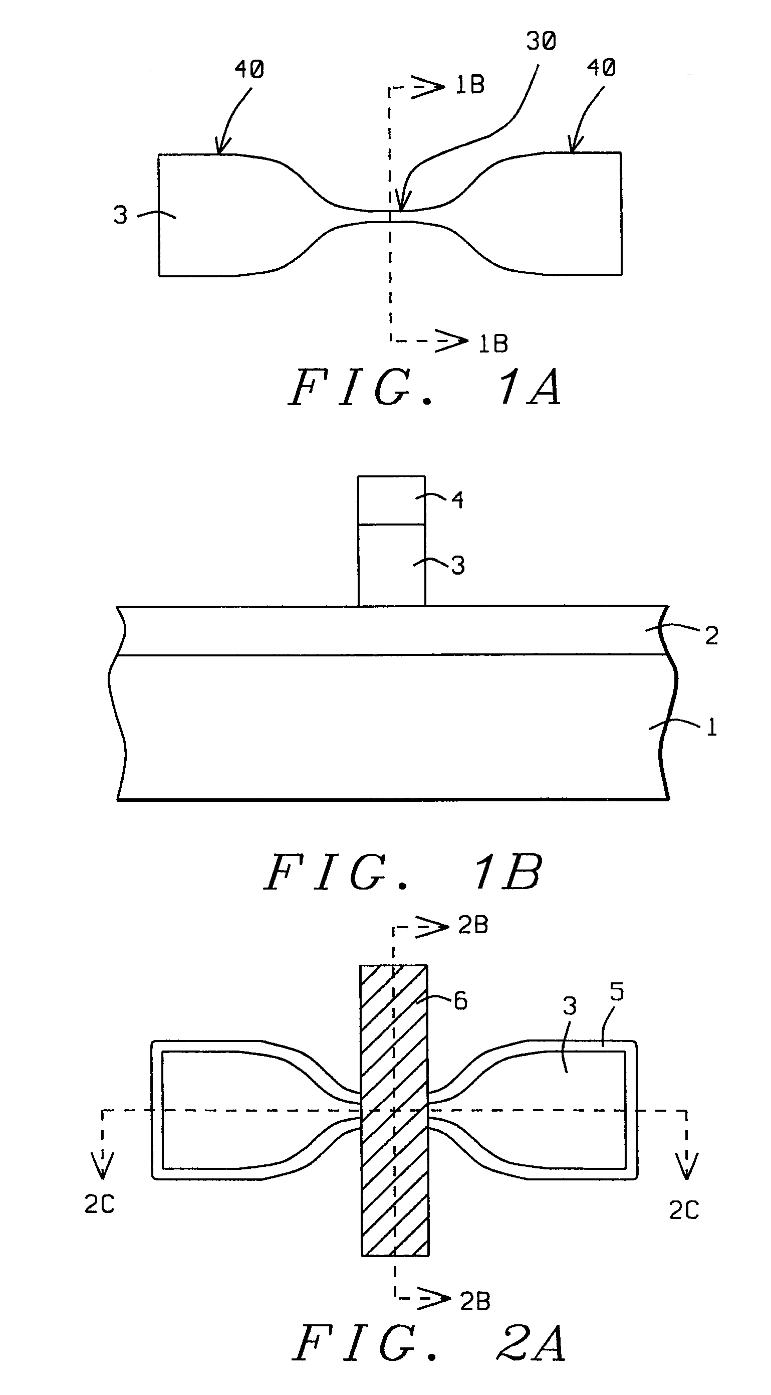
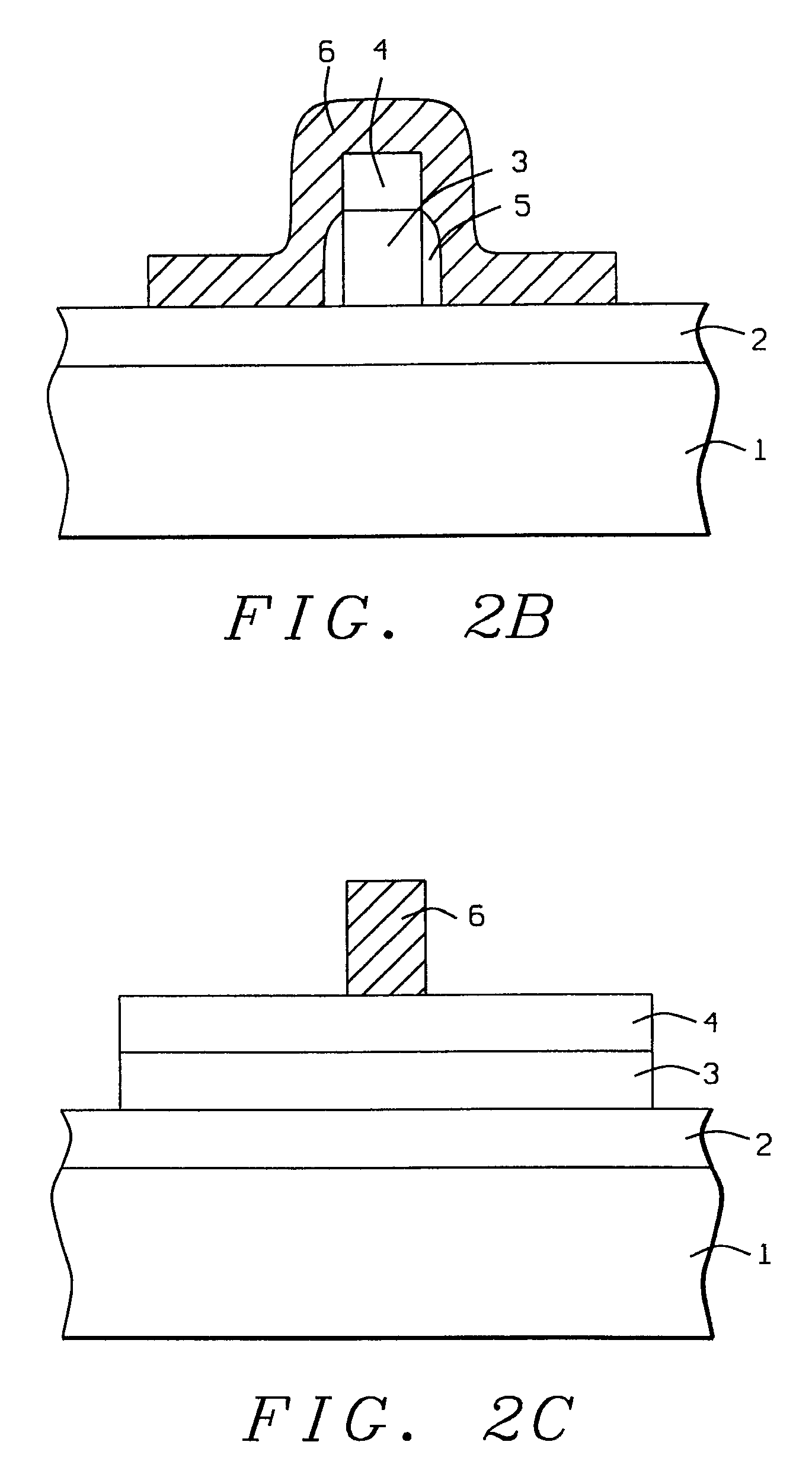
[0014] The method of fabricating a double gate FINFET device structure, defined in an SOI layer, wherein features such as a necked channel region and a wrap up insulator spacer are employed to reduce channel resistance and to prevent silicide formation on the sides of the FINFET device structure, will now be described in detail. Semiconductor substrate 1, comprised of single crystalline silicon with a crystallographic orientation, is used and schematically shown in cross-sectional style in FIG. 1B. Silicon layer 3, the silicon component of SOI layer 3, is formed via oxygen implantation into a portion of semiconductor substrate 1, followed by an anneal procedure which results in the formation of insulator layer 2, underlying an non-implanted, and non-oxidized silicon layer 3. Insulator layer 2, is comprised of silicon dioxide at a thickness between about 100 to 2000 Angstroms, while silicon layer 3, the top portion of semiconductor substrate 1, overlying insulator layer 2, is formed...


PUM


Abstract

A method of fabricating a double gate, FINFET device structure in a silicon on insulator layer, in which the channel region formed in the SOI layer is defined with a narrowed, or necked shape, and wherein a composite insulator spacer is formed on the sides of the device structure, has been developed. A FINFET device structure shape is formed in an SOI layer via anisotropic RIE procedures, followed by a growth of a silicon dioxide gate insulator layer on the sides of the FINFET device structure shape. A gate structure is fabricated traversing the device structure and overlying the silicon dioxide gate insulator layer located on both sides of the narrowest portion of channel region. After formation of a source / drain region in wider, non-channel regions of the FINFET device structure shape, composite insulator spacers are formed on the sides of the FINFET shape and on the sides of the gate structure. Metal silicide is next formed on source / drain regions resulting in a FINFET device structure featuring a narrow channel region, and surrounded by composite insulator spacers located on the sides of the device structure.

Description

RELATED APPLICATION [0001] This application is a divisional of U.S. patent application Ser. No. 10 / 835,789, filed Apr. 30, 2004, and entitled, “Method of Fabricating a Necked Finfet Device,” which is hereby incorporated by reference in its entirety.BACKGROUND OF THE INVENTION [0002] (1) Field of the Invention [0003] The present invention relates to methods used to fabricate semiconductor devices, and more specifically to a process sequence used top fabricate a FINFET device, a field effect transistor formed on an silicon on insulator (SOI) layer, with the mesa type device comprised with fin like features. [0004] (2) Description of Prior Art [0005] Micro-miniaturization, or the ability to fabricate semiconductor devices comprised with sub-micron features, have allowed performance increases for devices comprised with the sub-micron features to be realized, while the manufacturing cost of a specific semiconductor chip formed with sub-micron features has been reduced. The decrease in pe...

Claims


Application Information

Patent Timeline
Patent Type & Authority Applications(United States)
IPC IPC(8): H01L29/788H01L29/76H01L29/94H01L31/00H01L21/336H01L29/786
CPCH01L29/665H01L29/785H01L29/66795
Inventor CHEN, HAUR-YWHCHEN, FANG-CHENGCHAN, YI-LINGYANG, KUO-NANYANG, FU-LIANGHU, CHENMING
Owner TAIWAN SEMICON MFG CO LTD
Why Eureka
Try Eureka