Semiconductor device

a technology of semiconductors and devices, applied in the direction of pulse techniques, power conversion systems, instruments, etc., can solve the problems of increasing circuit scale and current consumption

Inactive Publication Date: 2007-03-22
KK TOSHIBA
View PDF15 Cites 31 Cited by
  • Summary
  • Abstract
  • Description
  • Claims
  • Application Information

AI Technical Summary

Benefits of technology

[0004] According to one aspect of the present invention, there is provided a semiconductor device including first and second switching elements connected in series between first and second terminals with a predetermined potential difference between the terminals, and a control unit which controls connection states of the first and second switching elements on the basis of an input signal such that when one of the first and second switching elements enters an off state, the other switching element enters an on state, wherein the control unit has a first drive unit to which a first reference potential is applied as a reference potential and which generates and outputs a first control signal for controlling the connection state of the first switching element on the basis of the input signal and a second control signal, a second drive unit to which a second reference potential different from the first reference potential is app

Problems solved by technology

However, implementation of high-speed operation involves problems such

Method used


Image

  • Semiconductor device
  • Semiconductor device
  • Semiconductor device

Examples


first embodiment

(1) First Embodiment

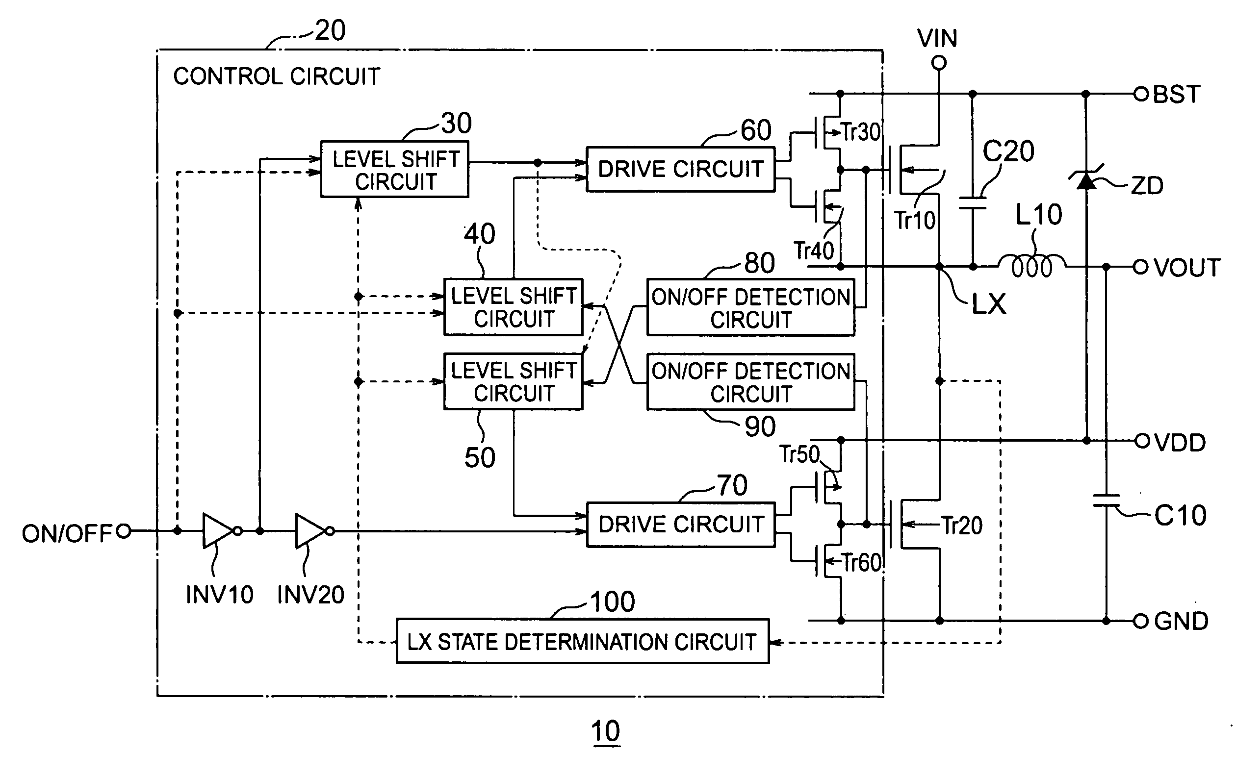
[0014]FIG. 1 shows the configuration of a DC-DC converter 10 according to a first embodiment of the present invention. The DC-DC converter 10 generates a desired level of DC voltage by converting a DC voltage input from a voltage input terminal VIN into a high-frequency AC voltage and smoothing the AC voltage and outputs the DC voltage from a voltage output terminal VOUT.

[0015] The DC-DC converter 10 has NMOS transistors Tr10 and Tr20 as switching elements. A source of the NMOS transistor Tr10 and a drain of the NMOS transistor Tr20 are connected, a drain of the NMOS transistor Tr10 is connected to the voltage input terminal VIN, and a source of the NMOS transistor Tr20 is connected to a ground terminal GND.

[0016] The DC-DC converter 10 alternates the operation of turning on or off the NMOS transistors Tr10 and Tr20 with the reverse operation such that if an NMOS transistor Tr, one of the NMOS transistors Tr10 and Tr20 is brought into an off state, the other NM...

second embodiment

(2) Second Embodiment

[0089]FIG. 6 shows the configuration of a DC-DC converter 300 according to a second embodiment of the present invention. Note that the same components as those shown in FIG. 1 are denoted by the same reference numerals and that an explanation thereof will be omitted. Level shift circuits 320 to 340 have the same configurations as the corresponding level shift circuits 30 to 50 (FIGS. 2 and 5) except for edge pulse circuits.

[0090] The potential of a node LX changes in response to a change in signals indicating the connection states of NMOS transistors Tr10 and Tr20 output from on / off detection circuits 80 and 90. Accordingly, in this embodiment, each of the level shift circuits 320 to 340 determines a time when an increased driving current is decreased using a signal notifying, of the connection state of one of the NMOS transistors Tr10 and Tr20, a drive circuit 70 or 60 for driving the other NMOS transistor Tr20 or Tr10, i.e., a signal output from the on / off de...

third embodiment

(3) Third Embodiment

[0102]FIG. 7 shows the configuration of a DC-DC converter 400 according to a third embodiment of the present invention. Note that the same components as those shown in FIG. 1 are denoted by the same reference numerals and that an explanation thereof will be omitted.

[0103] In this embodiment, a control circuit 410 has a drive circuit 480 for driving a PMOS transistor Tr50 and a drive circuit 490 for driving an NMOS transistor Tr60.

[0104] The drive circuits 480 and 490 are powered by different power sources. The drive circuit 490 uses, as a reference potential, 0 V, i.e., a low reference potential while the drive circuit 480 uses, as a reference potential, a potential between one applied from a power supply terminal VDD and 0 V (to be referred to as an intermediate reference potential hereinafter).

[0105] This makes it possible to increase the gate threshold voltage of an NMOS transistor Tr20 while maintaining the withstand voltages of the drive circuits 480 and ...


PUM


Abstract

According to this invention, there is provided a semiconductor device having conversion units which change the reference potential of an input signal to a first or second reference potential and outputs the input signal to a first drive unit or second drive unit, change the reference potential of a first control signal output from the first drive unit to the second reference potential and outputs the first control signal to the second drive unit, and changes the reference potential of a second control signal output from the second drive unit to the first reference potential and outputs the second control signal to the first drive unit, wherein the conversion units increase currents flowing through the conversion units on the basis of a time when the input signal changes.

Description

CROSS REFERENCE TO RELATED APPLICATIONS [0001] This application is based upon and claims benefit of priority under 35 USC 119 from the Japanese Patent Application No. 2005-258180, filed on Sep. 6, 2005, the entire contents of which are incorporated herein by reference. BACKGROUND OF THE INVENTION [0002] There are DC-DC converters which generate a desired level of DC voltage by converting an externally input DC voltage into a high-frequency AC voltage and smoothing the AC voltage and output the DC voltage to a subsequent circuit. A plurality of DC-DC converters of this type are mounted in, e.g., an electronic device such as a cellular phone handset which uses a battery as its power source and generate a plurality of voltages for respective functional blocks. [0003] In recent years, the operating frequencies of DC-DC converters have been increasing to cope with the lower voltage and higher current of a power source. For this reason, high-speed operation and high efficiency are require...

Claims


Application Information

Patent Timeline
IPC IPC(8): G05F1/00
CPCH02M1/38H03K2217/0036H03K17/165H03K17/04206
Inventor YOSHIKAWA, NORIAKI
Owner KK TOSHIBA
Why Eureka
Try Eureka