Transparent thin film transistor (TFT) and its method of manufacture

a thin film transistor and transparent technology, applied in the direction of basic electric elements, electrical equipment, semiconductor devices, etc., can solve the problems of difficult formation of ohmic contacts between source and drain electrodes and the transparent semiconductor activation layer, and achieve the effects of improving emission efficiency and stability, removing an energy barrier, and improving ohmic conta

Inactive Publication Date: 2007-03-29
SAMSUNG DISPLAY CO LTD
View PDF15 Cites 131 Cited by
  • Summary
  • Abstract
  • Description
  • Claims
  • Application Information

AI Technical Summary

Benefits of technology

[0033] According to the transparent TFT of the present invention and its method of manufacture, it is possible to remove an energy barrier which occurs when the transparent semiconductor activation layer contacts the electrodes so that it is possible to improve ohmic contact between the tra

Problems solved by technology

However, since transparent semiconductor materials that form the transparent semiconductor activation layer of the transparent TFT have a la

Method used


Image

  • Transparent thin film transistor (TFT) and its method of manufacture
  • Transparent thin film transistor (TFT) and its method of manufacture
  • Transparent thin film transistor (TFT) and its method of manufacture

Examples


Embodiment Construction

[0040] Hereinafter, exemplary embodiments of the present invention are described in detail with reference to the attached drawings. In this specification, the term “transparency” generally indicates not only relatively high transparency in which light having a wavelength of 300˜700 nm is transmitted by 50% or more, but also relatively low transparency in which the light is transmitted by 20 to 50%.

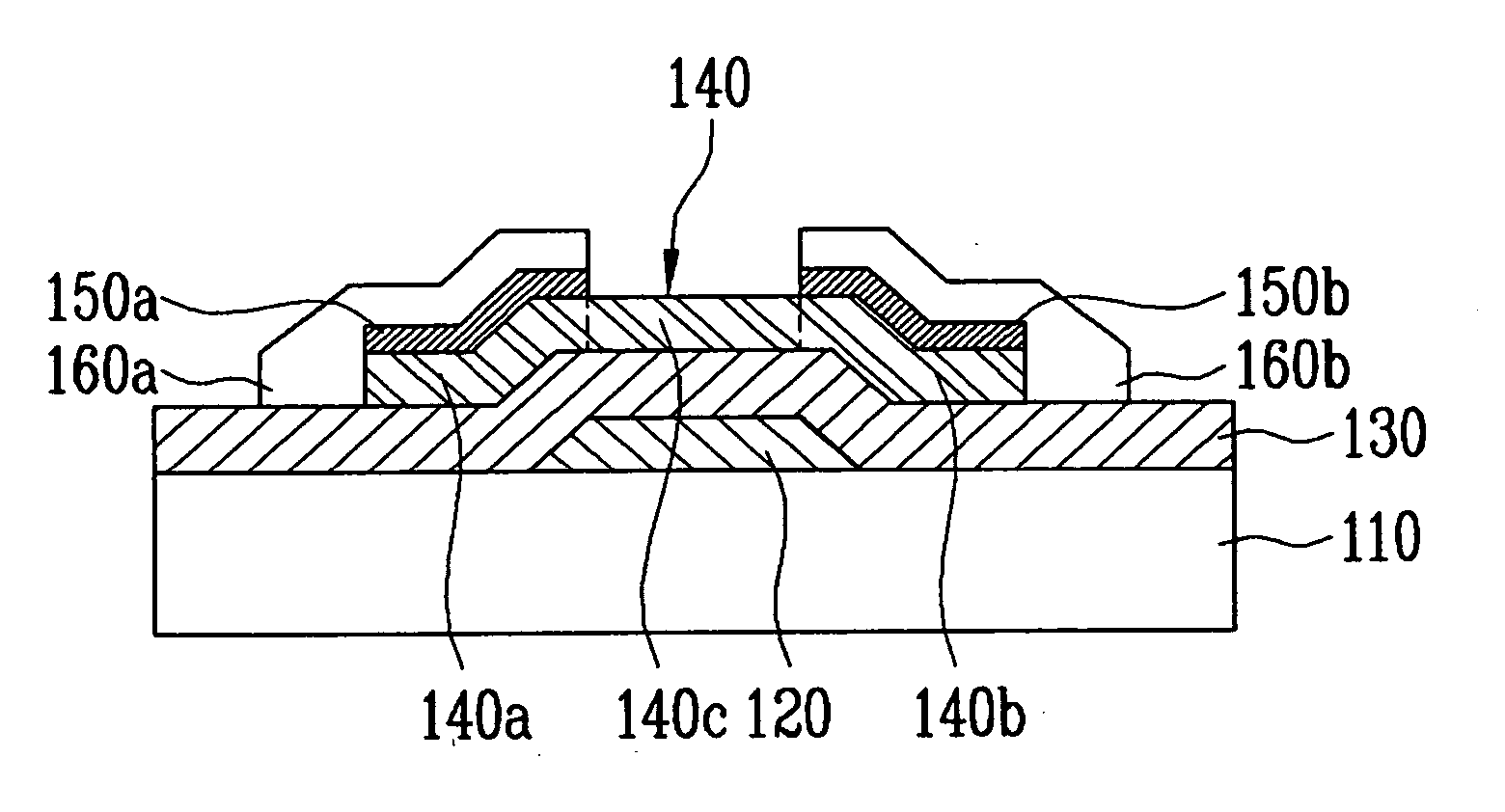
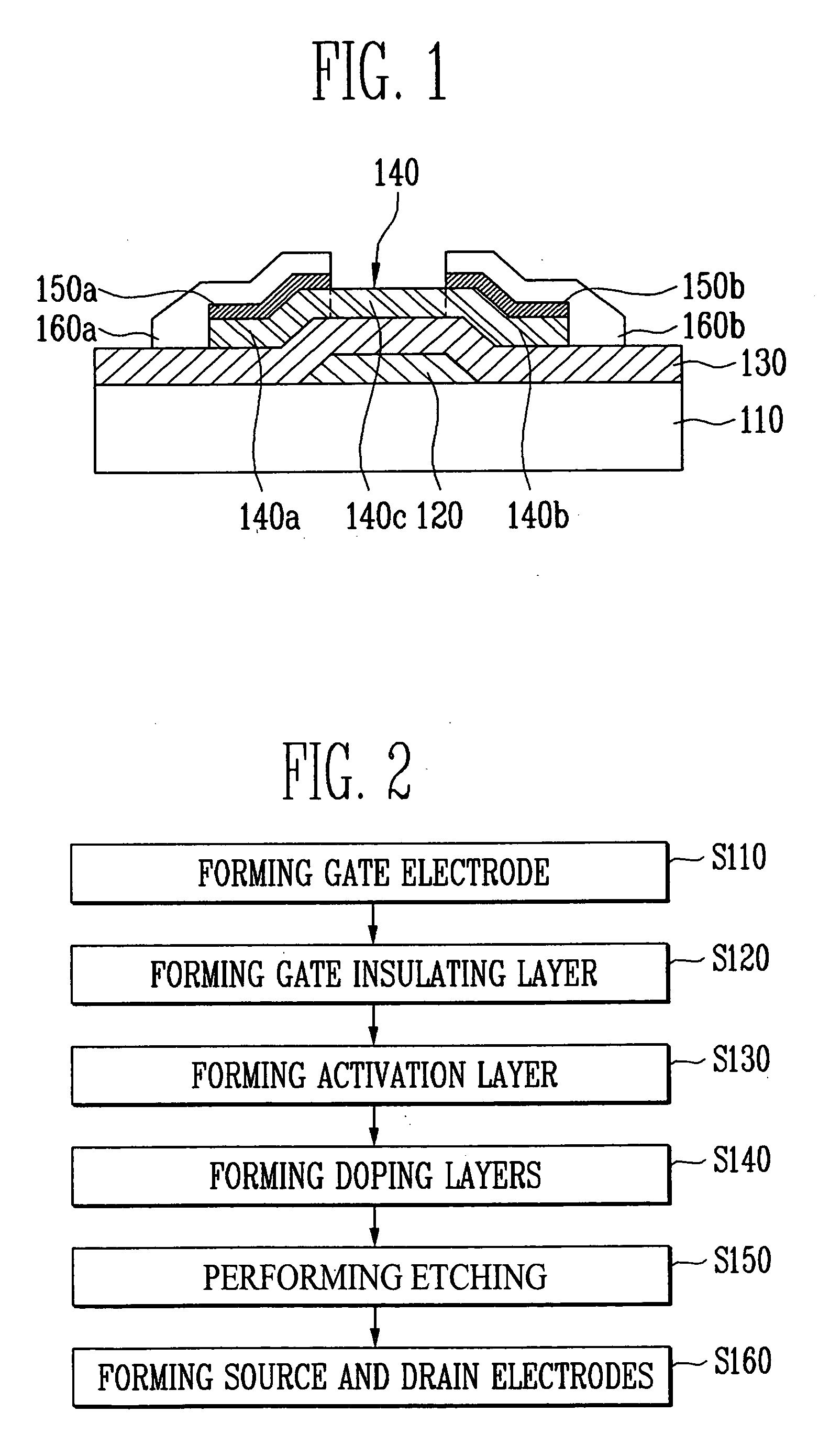
[0041]FIG. 1 is a sectional view of a bottom gate transparent Thin Film Transistor (TFT) according to a first embodiment of the present invention. Referring to FIG. 1, a transparent TFT includes a substrate 110, a gate electrode 120, a gate insulating layer 130, a transparent semiconductor activation layer 140, doping layers 150a and 150b and transparent source and drain electrodes 160a and 160b. Since the components of a common TFT are well known to one skilled in the art, the components that are related to the aspects of the present invention will be simply described.

[0042] The substra...


PUM


Abstract

A transparent thin film transistor (TFT) and a method of fabricating the same are provided. The transparent TFT includes transparent source and drain electrodes formed of transparent material, a transparent semiconductor activation layer that contacts the source and drain electrodes, that is formed of transparent semiconductor, and in which source and drain regions are formed, and a doping section provided between the transparent source and drain electrodes and the transparent activation layer to have the same doping type as that of the source and drain regions and to have doping concentration different from that of the source and drain regions. At this time, doping during the formation of the doping section is performed by an in-situ method in which a gas containing impurities is sprayed in the same apparatus as the apparatus used for the previous step. Therefore, it is possible to reduce high contact resistance generated when the transparent semiconductor activation layer contacts the transparent electrodes and to thus form ohmic contact.

Description

CLAIM OF PRIORITY [0001] This application makes reference to, incorporates the same herein, and claims all benefits accruing under 35 U.S.C. 119 from an application for TRANSPARENT THIN FILM TRANSISTOR AND MANUFACTURING METHOD THEREOF earlier filed in the Korean Intellectual Property Office on 27 Sep. 2005 and there duly assigned Serial No. 10-2005-0090134. BACKGROUND OF THE INVENTION [0002] 1. Field of the Invention [0003] The present invention relates to a transparent Thin Film Transistor (TFT) and its method of manufacture, and more particularly, to a transparent TFT in which an ohmic contact is formed between transparent electrodes and a transparent semiconductor activation layer. [0004] 2. Discussion of the Related Art [0005] A Thin Film Transistor (TFT) can be applied to a light emitting device, a smart window, and a solar battery so that studies on the TFT are actively performed. In order to make the TFT transparent, a substrate, electrodes, a transparent semiconductor activa...

Claims


Application Information

Patent Timeline
IPC IPC(8): H01L31/00
CPCH01L29/78621H01L29/7869H01L29/78681H01L29/458
Inventor JEONG, JAE-KYEONGSHIN, HYUN-SOOMO, YEON-GON
Owner SAMSUNG DISPLAY CO LTD
Why Eureka
Try Eureka