Solid-state imaging device and method for producing the same

a solid-state imaging and imaging device technology, applied in the direction of contact member manufacturing, television system, radioation controlled devices, etc., can solve the problems of high cost, inability to obtain a sufficient flatness of the base b>31, lens barrel not being aligned accurately with respect to the light-receptive region, etc., to achieve low cost, reduce variation in dimensional accuracy, and sufficient flatness

Inactive Publication Date: 2007-03-29
PANASONIC CORP
View PDF6 Cites 4 Cited by
  • Summary
  • Abstract
  • Description
  • Claims
  • Application Information

AI Technical Summary

Benefits of technology

[0012] Therefore, with the foregoing in mind, it is an object of the present invention to provide a solid-state imaging device whose base for mounting an imaging element has a practically sufficient flatness. In addition, it is another object of the present invention to provide a solid-state imaging device which is provided with wirings with a reduced variation in dimensional accuracy and at a low cost. Furthermore, it is still another object of the present invention to provide a manufacturing method that is suitable for producing such a solid-state imaging device.

Problems solved by technology

According to the configuration of the above-described conventional solid-state imaging devices, however, it is difficult to obtain a sufficient flatness of the base 31.
When the flatness of the face of the recess 33 to which the imaging element 35 is to be mounted is not sufficient, then the position of the imaging element 35 becomes unstable, resulting in the lens barrel not being aligned accurately with respect to the light-receptive region 35a.
In this respect, a process for applying the plating to the base 31 is complicated, and the process tends to generate a variation in dimensional accuracy of the formed wiring 34 and requires high cost.

Method used


Image

  • Solid-state imaging device and method for producing the same
  • Solid-state imaging device and method for producing the same
  • Solid-state imaging device and method for producing the same

Examples


embodiment 1

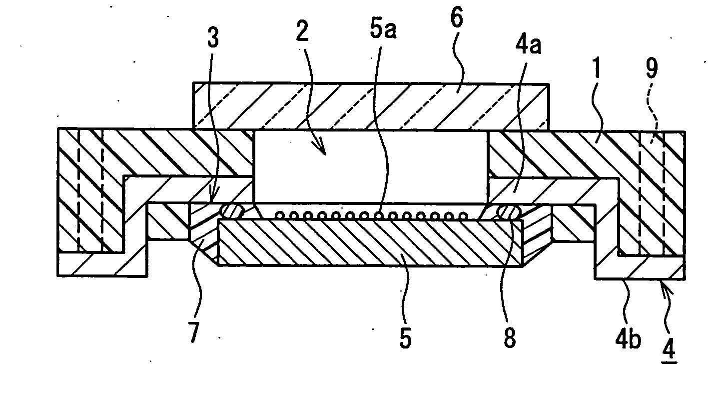
[0030] A solid-state imaging device of Embodiment 1 will be described below, with reference to FIGS. 1 and 2. A base 1 is made of a plastic resin such as an epoxy resin and has a rectangular frame form in planar shape having a rectangular aperture 2 in its center portion. A bottom face of the base 1 is recessed at a region along a periphery of the aperture 2 so as to form a rectangular recess 3 that surrounds the aperture 2. The bottom face of the base 1 is provided with a plurality of wirings 4 made of thin metal plate leads, which extend from the vicinity of the aperture 2 to an outer peripheral end face of the base 1. As the thin metal plate leads, Cu alloy, 42 alloy (Fe—Ni 42 alloy) and the like, which are similar to the materials used for a normal lead frame, are used. Thickness thereof usually ranges approximately from 2 to 3 μm.

[0031] On the surface of the recess 3 with the wirings 4 formed thereon, an imaging element 5 such as a CCD and the like formed on a Si base is mount...

embodiment 2

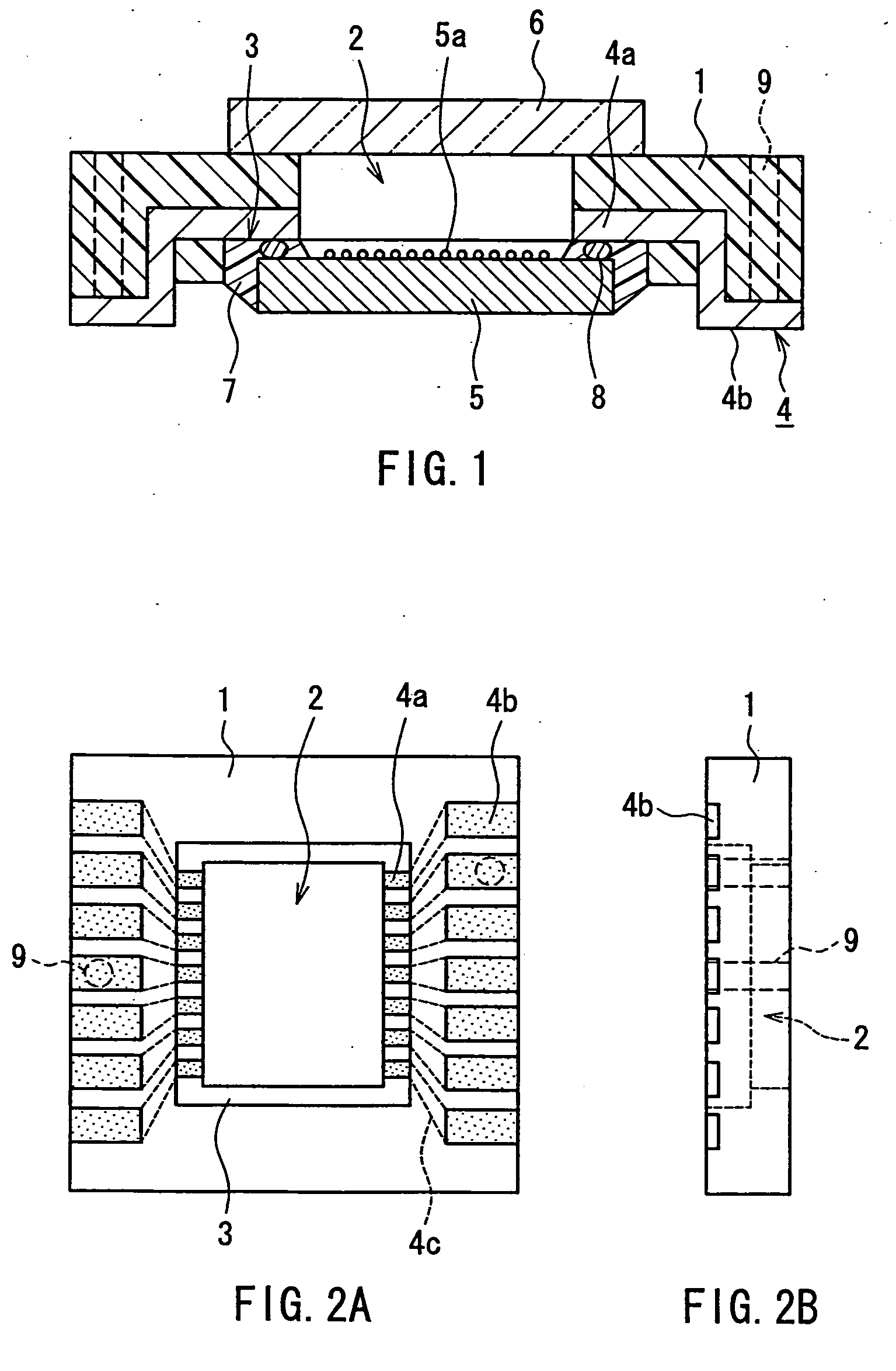
[0039] A solid-state imaging device according to Embodiment 2 will be described below, with reference to FIGS. 3 and 4. The same reference numerals will be assigned to the same elements as in Embodiment 1 so as to simplify their explanations. This embodiment is different from Embodiment 1 in the configuration of a base 10. The base 10 with a rectangular planar shape has a flat plate form having a uniform thickness as the whole in its cross-sectional shape, and does not have a recess as in Embodiment 1. An aperture 11 is formed in the central portion of the plate form base 10, and an imaging element 5 is mounted thereon with its light-receptive region 5a facing the aperture 11.

[0040] On the bottom face of the base 10, a plurality of wirings 12 made of thin metal plate leads are disposed, which extend from the edge of the aperture 11 to an outer peripheral end face of the base 10. On an electrode pad (not illustrated) disposed on the same surface of the imaging element 5 as the light...

embodiment 3

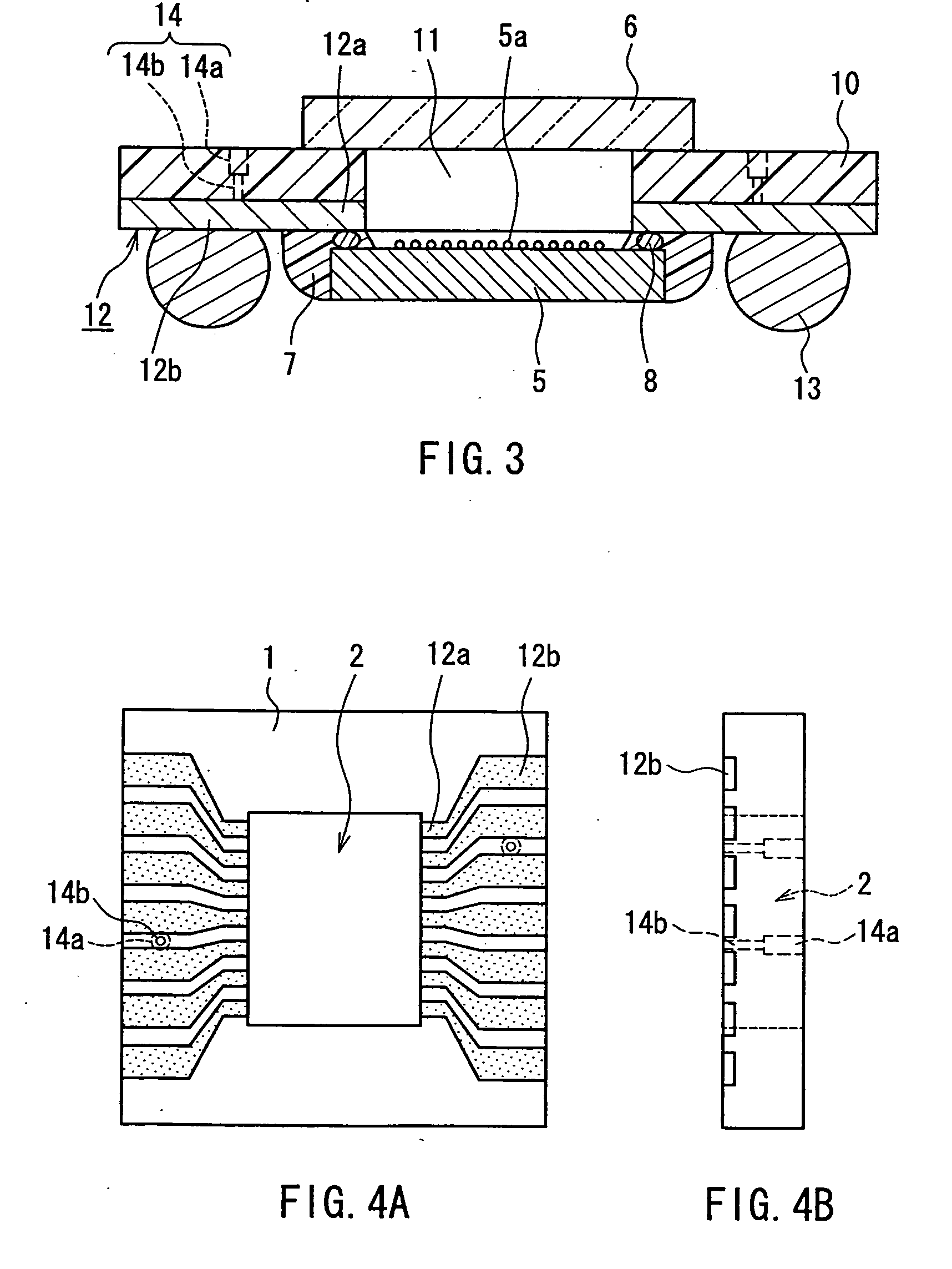
[0044] A method for producing the solid-state imaging device having the above-described configurations will be described below, with reference to FIGS. 5 and 6. In the following description, a case where the manufacturing method of this embodiment is applied for manufacturing the solid-state imaging device having the configuration of FIGS. 1 and 2, will be exemplified. FIGS. 5A to 5C show only a process of molding a base. FIG. 6 is a plan view of the base at a stage of FIG. 5B.

[0045] Firstly, a lower mold 20 and an upper mold 21 shown in FIG. 5A are prepared as molds for resin molding. The lower mold 21 has a recess 20aformed therein. This recess is filled with a resin so as to mold the base 1 of FIG. 1. Note here that FIG. 5A shows the base 1 being molded by turning the state of FIG. 1 upside down. In the central portion of the lower mold 20, a lower protrusion 20b also is formed. The upper mold 21 has an upper protrusion 21a formed in its central portion. When the lower mold 20 a...


PUM

PropertyMeasurementUnit
shapeaaaaaaaaaa
transparentaaaaaaaaaa
areaaaaaaaaaaa

Abstract

A solid-state imaging device includes: a base made of an insulation material and having a frame form in planar shape with an aperture formed at an inner region; a plurality of wirings provided on one surface of the base and extending toward an outer periphery of the base from a region along the aperture; and an imaging element mounted on the surface of the base with wirings provided thereon so that a light-receptive region of the imaging element faces the aperture. An end portion on the aperture side of each of the plurality of wirings forms an internal terminal portion and an end portion on the outer peripheral side of each of the plurality of wirings forms an external terminal portion, the internal terminal portion of the wiring being connected electrically with an electrode of the imaging element. The wirings are made of thin metal plate leads, the base is made up of a resin molded member in which the thin metal plate leads are embedded, and at least a part of a side edge face of the thin metal plate leads is embedded in the base. The rigidity of the base is enhanced by the thin metal plate leads, thus reducing a curl and a warp of the base.

Description

[0001] This application is a Division of U.S. Ser. No. 10 / 676,135, filed Sep. 30, 2003, which application is incorporated herein by reference.BACKGROUND OF THE INVENTION [0002] 1. Field of the Invention [0003] The present invention relates to solid-state imaging device configured by mounting an imaging element such as a CCD on a base and a method for producing the same. [0004] 2. Related Background Art [0005] Solid-state imaging devices are used widely for video cameras and still cameras, and are provided in a form of a package in which an imaging element such as a CCD is mounted on a base made of an insulating material and a light-receptive region is covered with a transparent plate. In order to miniaturize the device, the imaging element is mounted on the base while keeping a bare chip state (for example, see JP 2000-58805 A). Such a conventional example of the solid-state imaging devises will be described below with reference to FIG. 7. [0006] A base 31 in FIG. 7 is made of ceram...

Claims


Application Information

Patent Timeline
Patent Type & Authority Applications(United States)
IPC IPC(8): H01L31/0203H01K3/22H01R43/00H01L27/14H01L23/00H01L23/04H01L27/146H01L27/148H04N5/335
CPCH01L27/14618H01L2224/16225Y10T29/4922Y10T29/49158Y10T29/49176Y10T29/49167Y10T29/49121Y10T29/49204H01L2924/00014H01L2224/0401H01L23/00H01L27/148
Inventor MINAMIO, MASANORITSUJI, MUTSUOYAMAUCHI, KOUICHI
Owner PANASONIC CORP
Why Eureka
Try Eureka