

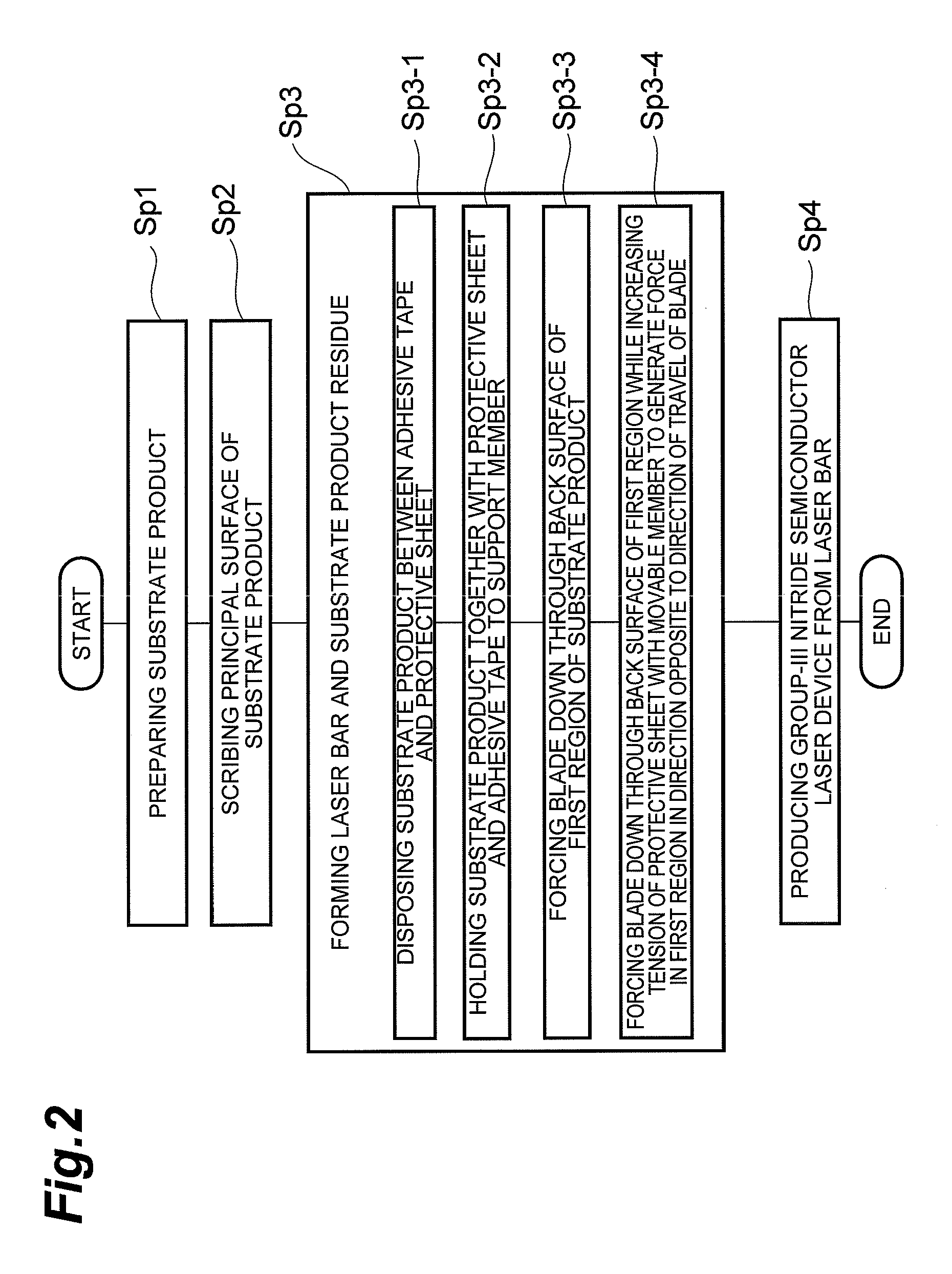
Method for fabricating group-iii nitride semiconductor laser device
a technology of semiconductor lasers and nitride, which is applied in semiconductor lasers, electrical devices, nanooptics, etc., can solve the problem that cavity mirrors orthogonal to laser waveguides cannot be readily produced, and achieve high flatness and perpendicularity
- Summary
- Abstract
- Description
- Claims
- Application Information
AI Technical Summary
Benefits of technology
Problems solved by technology
Method used
Image

Examples
example
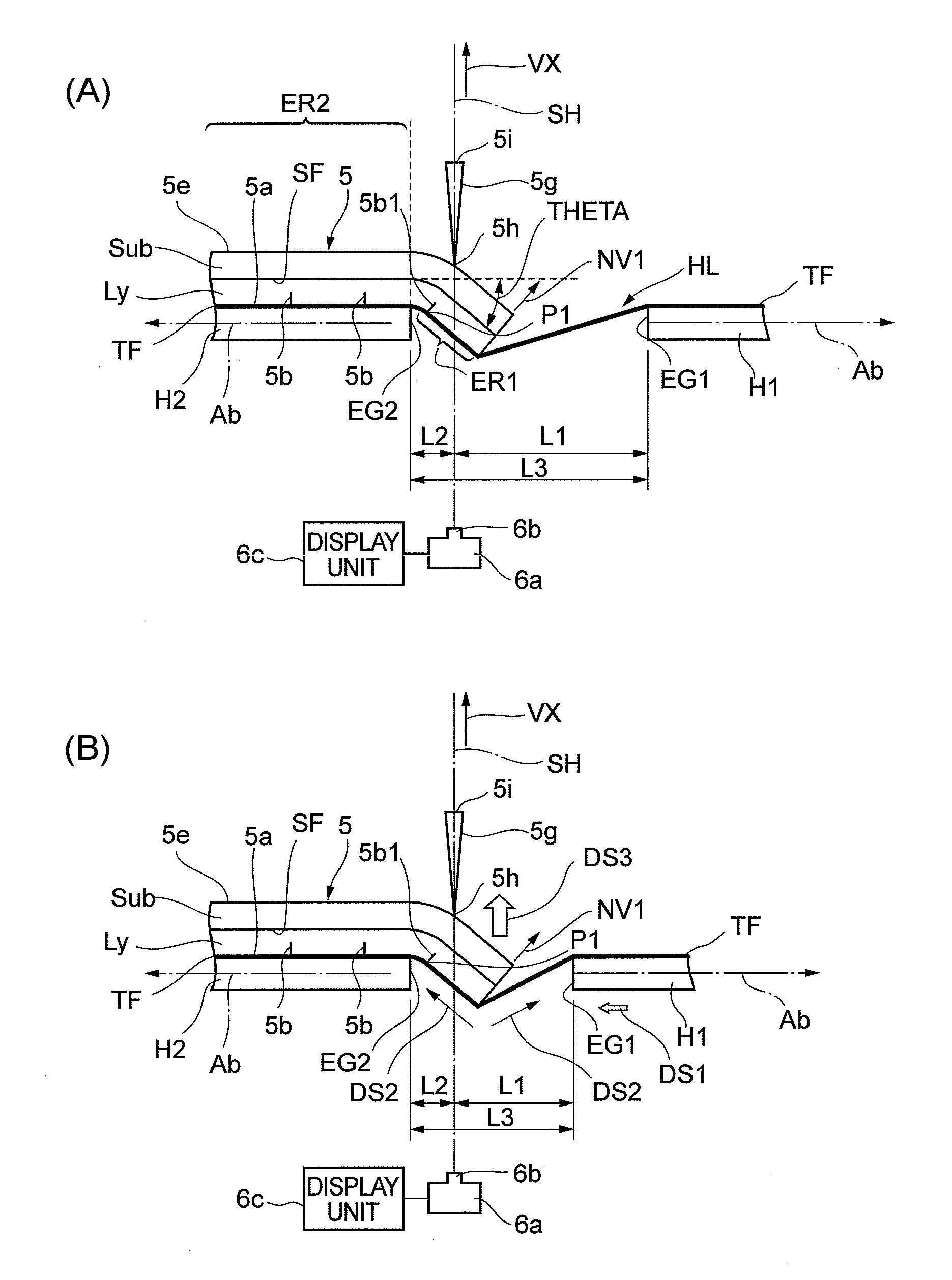
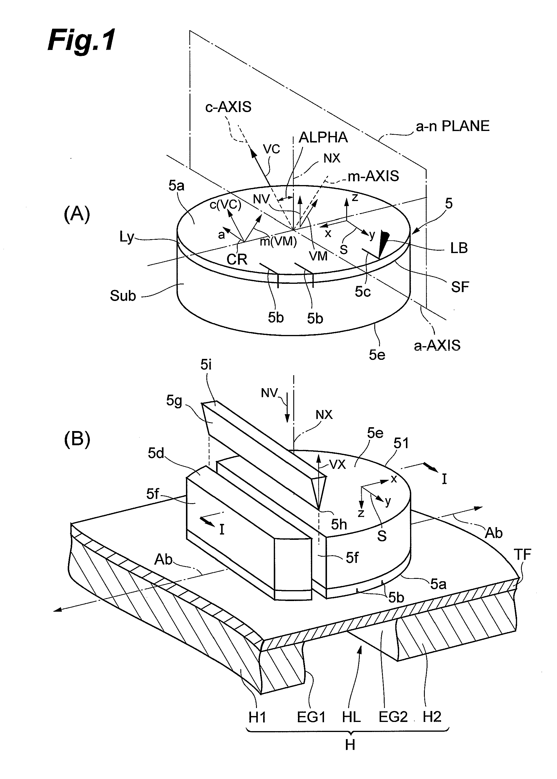
[0102]A laser diode is fabricated through organometallic vapor phase epitaxy, as illustrated in FIG. 9. The laser diode illustrated in FIG. 9 corresponds to the group-III nitride semiconductor laser device 11 illustrated in FIG. 7. The materials used are trimethyl gallium (TMGa), trimethyl aluminum (TMAl), trimethyl indium (TMIn), ammonium (NH3), and silane (SiH4). The substrate is a GaN substrate (corresponding to the substrate Sub and the support base 17) having a principal surface of the (20-21) plane cutout from a thick (0001) GaN ingot that is grown by HVPE at an angle of 75 degrees toward the m-axis. The substrate is placed on a susceptor in the reactor, and an epitaxial layer (corresponding to the semiconductor region Ly and the semiconductor region 19) is grown through the following procedures.
[0103]An n-type GaN layer (corresponding to the semiconductor layer 20) is grown into a thickness of approximately 1000 nm. An n-type InAlGaN layer (corresponding to the n-side claddin...
PUM
 Abstract
Description
Claims
Application Information