Image sensor module, camera module using the same, and method of manufacturing the camera module

a technology of image sensor and camera module, which is applied in the direction of circuit optical details, printed circuit aspects, television systems, etc., can solve the problems of increasing the need for additional processes, and the cost of the process, so as to reduce the percent of defective related to high resolution and resolution, prevent the optical axis shifting, tilting and rotation, and reduce the size of the module

Inactive Publication Date: 2007-03-29
SAMSUNG ELECTRO MECHANICS CO LTD
View PDF8 Cites 14 Cited by
  • Summary
  • Abstract
  • Description
  • Claims
  • Application Information

AI Technical Summary

Benefits of technology

[0025] An advantage of the present invention is that it provides an image sensor module and a camera module using the same, in which an optical axis passing through a lens section is accurately positioned in a light receiving section of an image sensor, thereby preventing optical axis shifting, tilting, and rotation. Therefore, percent defective related to high resolution and resolution can be reduced, and the size of the module can be reduced to achieve the miniaturization.
[0026] Another advantage of the invention is that it provides a method of manufacturing the camera module.
[0027] Additional aspects and advantages of the present general inventive concept will be set forth in part in the description which follows and, in part, will be obvious from the description, or may be learned by practice of the general inventive concept.
[0028] According to an aspect of the invention, an image sensor module includes a flexible printed circuit board (FPCB) having a window; and an image sensor that is formed to have the same size as the width of the FPCB and is attached on one surface of the FPCB, the image sensor including a light receiving section, which receives light passing through the window, and a signal processing section which processes signals generated by the light receiving section.
[0029] According to another aspect of the invention, the FPCB is a rigid flexible printed circuit board (RFPCB) or a double-sided flexible printed circuit board (FPCB).
[0030] According to a further aspect of the invention, at least one more electrical part is attached on the other surface of the FPCB having the image sensor attached thereon.

Problems solved by technology

However, since wire should be used for the connection with a PCB, the size of a module increases and an additional process is needed.
However, the process cost thereof is expensive, and the correspondence to the due date is unstable.
Therefore, the method has a limit as a method for image sensor.
In such techniques, however, the degree of difficulty in design is high, and process management is not easy.
In such a COB packaging method, three types of tolerances are generated, and thus an optical axis passing through the lens section is not accurately positioned in a light receiving section of the image sensor.
In such a COF packaging method, two types of tolerances are generated so that the optical axis passing through the lens section is not accurately positioned in a light receiving section of the image sensor.
As a result, the size of a required FPCB becomes so large that the overall size of the image sensor module becomes large.
At this time, if the multilayer ceramic capacitor is removed from the image sensor module, screen noise occurs.
However, such problems are inevitable in order to reduce the overall size of the camera module including the housing.

Method used


Image

  • Image sensor module, camera module using the same, and method of manufacturing the camera module
  • Image sensor module, camera module using the same, and method of manufacturing the camera module
  • Image sensor module, camera module using the same, and method of manufacturing the camera module

Examples


Embodiment Construction

[0052] Reference will now be made in detail to the embodiments of the present general inventive concept, examples of which are illustrated in the accompanying drawings, wherein like reference numerals refer to the like elements throughout. The embodiments are described below in order to explain the present general inventive concept by referring to the figures.

[0053] Hereinafter, preferred embodiments of the present invention will be described in detail with reference to the accompanying drawings.

[0054] [Image Sensor Module and Camera Module]

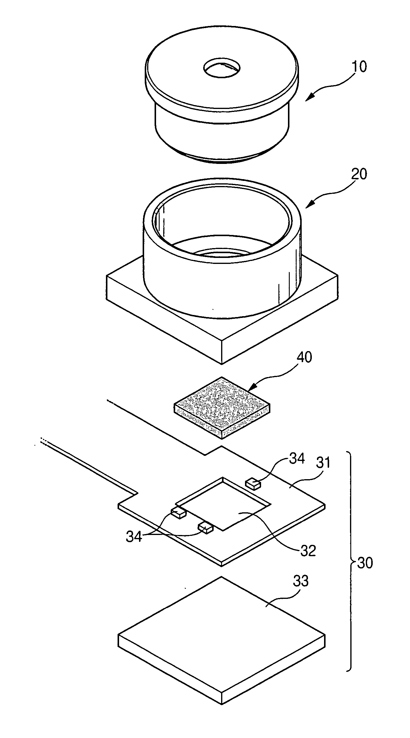
[0055]FIG. 3 is an exploded perspective view of a camera module including an image sensor module according to the invention, and FIG. 4 is a sectional view of the camera module.

[0056] As shown in FIGS. 3 and 4, the camera module according to the invention is composed of a lens section 10, a housing 20 into which the lens section 10 is inserted from the upper opening thereof so as to be mounted, and an image sensor module 30 which is coupled to...


PUM


Abstract

The present invention relates to an image sensor module including a flexible printed circuit board (FPCB) having a window; and an image sensor that is formed to have the same size as the width of the FPCB and is attached on one surface of the FPCB, the image sensor including a light receiving section, which receives light passing through the window, and a signal processing section which processes signals generated by the light receiving section.

Description

CROSS-REFERENCE TO RELATED APPLICATIONS [0001] The application claims the benefit of Korea Patent Application No. 2005-0089837 filed with the Korea Intellectual Property Office on Sep. 27, 2005, the disclosure of which is incorporated herein by reference. BACKGROUND OF THE INVENTION [0002] 1. Field of the Invention [0003] The present invention relates to an image sensor module, which is used in digital cameras, mobile equipments, various monitoring devices or the like, a camera module using the same, and a method of manufacturing the camera module. In the image sensor module, process tolerance generated by an existing packaging method is minimized to prevent an optical axis from being shifted, which makes it possible to improve productivity. [0004] 2. Description of the Related Art [0005] As the information communication technology rapidly develops, data communication speed is improved, and an amount of data communication is expanded. Further, an imaging device such as a CCD image s...

Claims


Application Information

Patent Timeline
Patent Type & Authority Applications(United States)
IPC IPC(8): H01L23/48H01L27/14H04N5/225H04N5/335H04N5/369
CPCH01L27/14618H01L27/14625H01L27/14685H05K2201/10121H05K1/0274H05K1/189H05K2201/09072H04N5/2257H01L2924/0002H04N23/57H01L2924/00H04N23/00
Inventor KIM, HO KYOUMKWAK, HYUNG CHANSHIN, DONG MIN
Owner SAMSUNG ELECTRO MECHANICS CO LTD
Why Eureka
Try Eureka