Shift register circuit and display apparatus using the same

Active Publication Date: 2007-03-29
PANASONIC LIQUID CRYSTAL DISPLAY CO LTD +1
View PDF10 Cites 56 Cited by
  • Summary
  • Abstract
  • Description
  • Claims
  • Application Information

AI Technical Summary

Benefits of technology

[0015] According to the invention, particularly, as shown in FIG. 11, the GDC holding device control circuit 18 is constructed by a setting device T9, a resetting device T10, and a holding capacitor C3. An output from a fundamental circuit of two stages before is inputted to a gate terminal of the resetting device T10. Thus, the GDC holding device T8 can be certainly turned off before the GDC charging device T4 is turned on. The generation of the wasteful through-current can be prevented.
[0016] According to the invention, particularly, as shown in FIG. 14, the shift register circuit is arranged to both sides of the display apparatus, so that the output of the funda

Problems solved by technology

It has been known that a similar problem occurs not only in the a—Si TFT but also in an organic TFT or the like.
If the driving ability of the TFT deteriorates, upon preparation for

Method used


Image

  • Shift register circuit and display apparatus using the same
  • Shift register circuit and display apparatus using the same
  • Shift register circuit and display apparatus using the same

Examples


Example

Embodiment 1

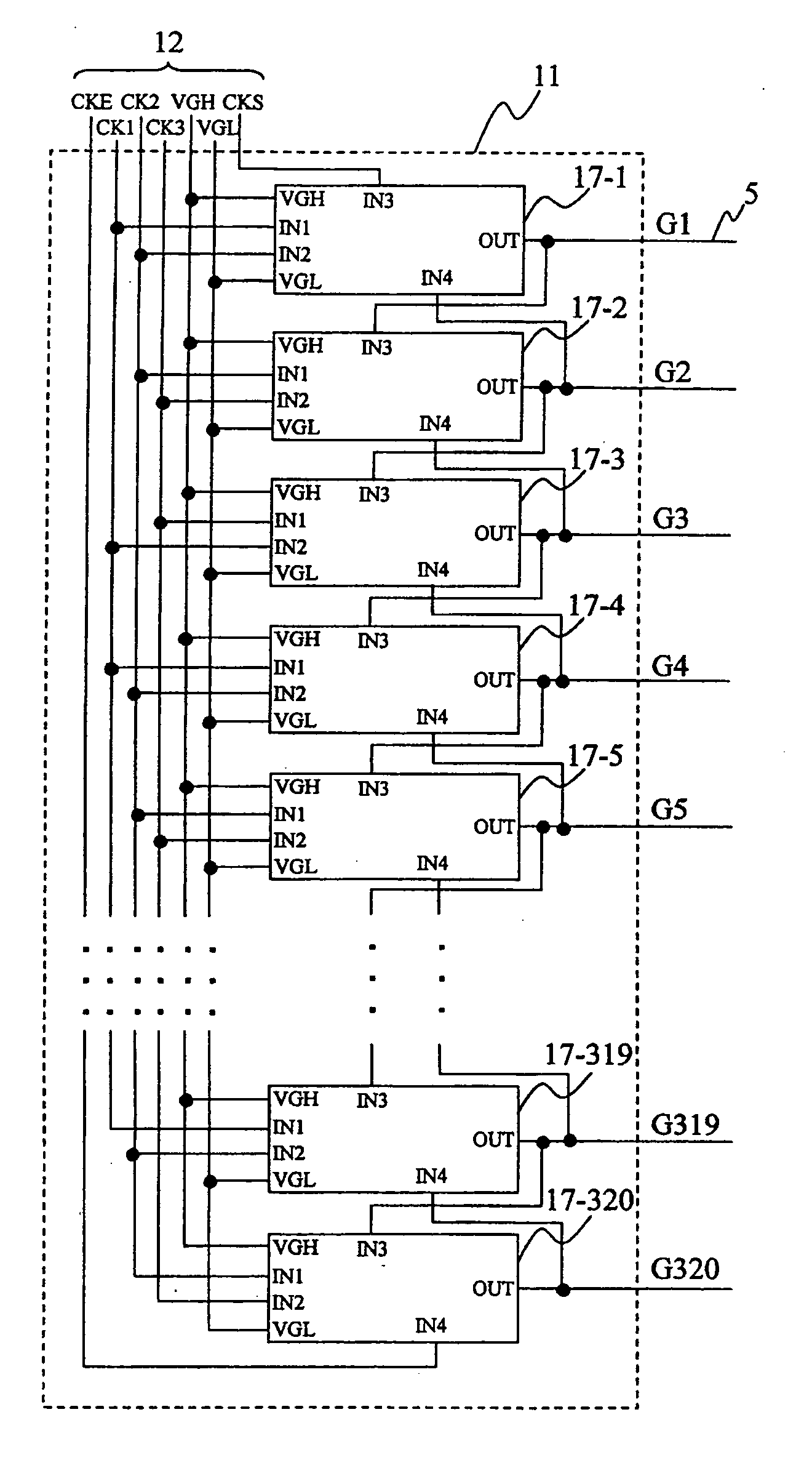
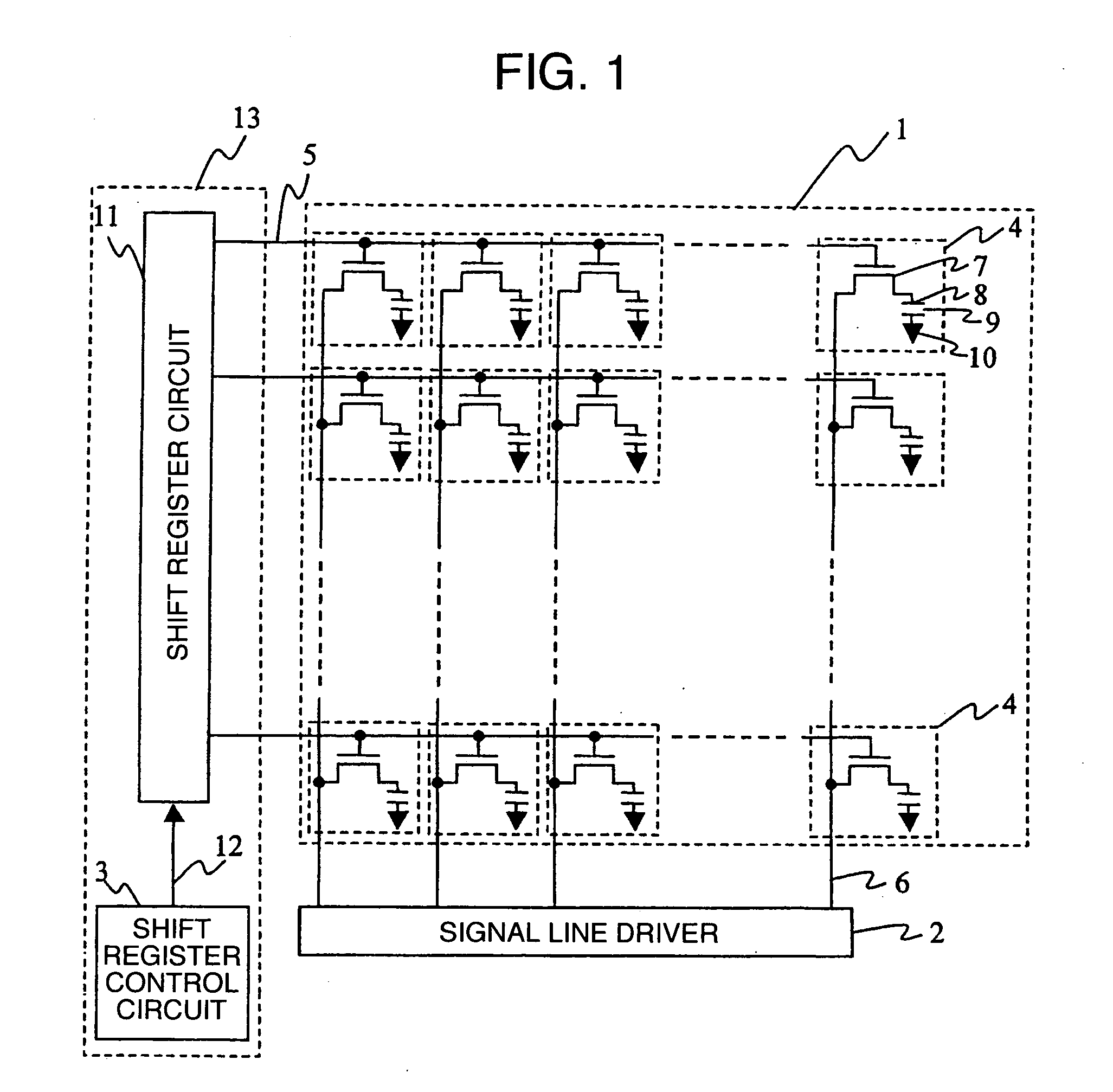
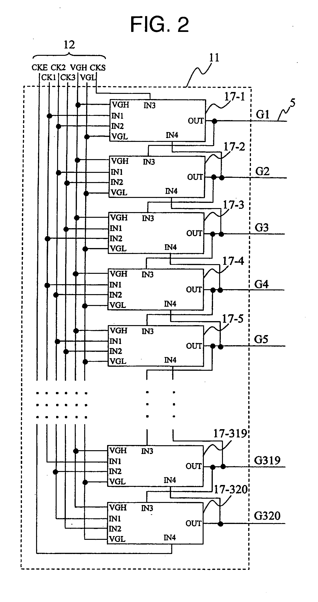
[0034]FIG. 1 is a schematic diagram showing a whole construction of a display apparatus according to the present invention. The display apparatus is constructed by a display unit 1, a signal line driver 2, and a gate line driver 13. Pixel portions 4 are arranged in a matrix form in the display unit 1 formed on a glass substrate. Each of the pixel portions 4 has a structure in which a thin film transistor (TFT) 7 exists in a crossing portion of a signal line 6 and a gate line 5. The gate line 5 is connected to a gate terminal of the TFT 7, the signal line 6 is connected to a first terminal, a pixel electrode 8 is connected to a second terminal. Although the first terminal and the second terminal of the TFT will be separately explained, there is no difference between functions of them.

[0035] In the display apparatus of the embodiment, it is assumed that there are 720 (=240×RGB) signal lines 6 and there are 320 gate lines 5. A liquid crystal layer 9 is sandwiched between ...

Example

Embodiment 2

[0087] In the example shown in FIG. 3, the gate line holding device T2 and the GDC holding device T8 are controlled by using one holding device control circuit 16. However, as shown in FIG. 9, it is also possible to construct the holding device control circuit 16 by two control circuits such as first and second holding device control circuits; that is, a gate line holding device control circuit 19 for controlling the gate line holding device T2; and a GDC holding device control circuit 18 for controlling the GDC holding device T8. Since each of the gate line holding device control circuit 19 and the GDC holding device control circuit 18 has a structure and an operation principle similar to those of the holding device control circuit 16-3 or a holding device control circuit 16-3′ shown in FIG. 4 or 6, their detailed explanation is omitted here.

Example

Embodiment 3

[0088] In the fundamental circuit 17 shown in FIG. 3, the GDC holding device T8 is turned by such a procedure that the third input terminal IN3 is set to the H level, the resetting device T7 is turned on, so that the charges in the holding capacitor C2 are discharged, and the GDC holding device T8 is turned off. However, to turn on the GDC charging device T4, it is sufficient that the third input terminal IN3 is set to the H level. Therefore, such a situation that before the GDC holding device T8 is set to the sufficient OFF state, the GDC charging device T4 is turned on is considered. If such a state occurred, the current flows momentarily from the high-level voltage VGH toward the low-level voltage VGL, so that it is undesirable. To certainly prevent such a situation, it is necessary that the GDC holding device T8 has certainly been set to the OFF state before the GDC charging device T4 is turned on. An embodiment in such a case will be shown below.

[0089]FIG. 10 is a...


PUM


Abstract

A shift register circuit which stably operates with low electric power consumption and can realize a long life. In the shift register circuit constructed by connecting a plurality of fundamental circuits in each of which fundamental clocks of three phases are inputted to input terminals and is constructed by a gate line driving circuit, a timing control circuit, and a holding device control circuit, each of the gate line driving circuit and the timing control circuit has charging devices and holding devices. A node is stabilized by the timing control circuit.

Description

INCORPORATION BY REFERENCE [0001] The present application claims priority from Japanese application JP 2005-284392 filed on Sep. 29, 2005, the content of which is hereby incorporated by reference into this application. BACKGROUND OF THE INVENTION [0002] 1. Field of the Invention [0003] The invention relates to a shift register circuit and a display apparatus using such a circuit and, more particularly, to an LCD (Liquid Crystal Display) or a TFT (Thin Film Transistor) active matrix display. [0004] 2. Description of the Related Art [0005] Hitherto, in an amorphous silicon (a—Si) TFT-LCD, in order to reduce fabrication costs and driving IC costs, improve the reliability, and reduce an area of a non-display portion, a shift register built-in type system in which a shift register circuit for scanning gate lines is integrated simultaneously with TFTs of a pixel portion and mounted has been proposed. As a typical example of such a system, for example, JP-A-2004-348940 can be mentioned. [0...

Claims


Application Information

Patent Timeline
IPC IPC(8): G09G3/36
CPCG09G3/20G09G3/3677G09G2300/0417G11C19/184G09G2310/08G09G2330/021G09G2310/0267
Inventor EDO, SUSUMUKOMURA, SHINICHIWAKAGI, MASATOSHI
Owner PANASONIC LIQUID CRYSTAL DISPLAY CO LTD
Why Eureka
Try Eureka