Semiconductor device with improved design freedom of external terminal

a technology of external terminals and semiconductors, applied in the field of semiconductor devices, can solve the problems of difficult to form 300 external terminals on the surface area of a 7 mm7 mm wcsp, severe restriction of design freedom, and large volume of external electrodes, etc., and achieve the effect of compactness, and increasing the number of functions

Active Publication Date: 2007-03-29
LAPIS SEMICON CO LTD
View PDF3 Cites 7 Cited by
  • Summary
  • Abstract
  • Description
  • Claims
  • Application Information

AI Technical Summary

Benefits of technology

[0028] According to the constitution of the semiconductor device of this invention, external terminals can also be provided on the upper side of the extension portion which is provided in contact with and surrounding the semiconductor chip, and thus a semiconductor device having increased design freedom in the disposal pitch, disposal positions, and so on of the external electrodes can be provided. Further, the semiconductor device of this invention may be constructed without the use of an interposer such as a substrate by applying a so-called WCSP manufacturing process, as a result of which increases in operating speed, functional sophistication, number of functions, and compactness can be achieved in comparison with a wire bonding connection. Moreover, an identical electrical characteristic can be obtained at a lower cost than a device in which a flip chip connection is used.
[0029] Moreover, the semiconductor device of this invention is capable of dispersing heat generated by the semiconductor chip into the atmosphere surrounding the semiconductor chip via the base which is formed in consideration of thermal radiation, and thus defects such as malfunctions caused by heat can be prevented.
[0096] According to this manufacturing method for the semiconductor device of this invention, a semiconductor device with increased functional sophistication, number of functions, and compactness can be provided by means of a comparatively easy process. In particular, design freedom in the disposal pitch, disposal positions, and so on of the external electrodes can be greatly increased.
[0097] Further, the construction for aiding singularization is formed on the base from one, two, or more groove portions or a plurality of through holes, for example, and thus the singularization process of the semiconductor device can be performed extremely easily.
[0098] Particularly when the base is formed from a metallic material, for example, in consideration of thermal conductivity and thermal radiation, the amount of burrs (shavings) of the metallic material, which are inevitably produced during implementation of the singularization process, can be reduced. Accordingly, electrical short circuits caused when the burrs of the metallic material become attached between circuits on the mounting substrate or between terminals on electronic components, and defects such as malfunctions caused by these short circuits can be reduced greatly. Irregularities in the outer form of the manufactured semiconductor devices can also be reduced.
[0099] Further, from among the cutting devices used in the singularization process, wear in a blade which cuts the base while in contact therewith can be further reduced, and thus the effect of a further reduction in the manufacturing costs of the semiconductor device can be expected.

Problems solved by technology

As shall be described below, however, design freedom is severely restricted by the disposal pitch and disposal positions of external terminals.
However, it is extremely difficult to form 300 external terminals on the surface area of a 7 mm×7 mm WCSP.
Since both of these connection methods utilize a substrate, and since additional sealing material is required in accordance with the height of the wire loop, the package becomes thick.
Moreover, the package becomes expensive due to the cost of the substrate.
The package becomes particularly expensive when a flip chip connection is used since an expensive buildup substrate is required.
When peripheral structures and the semiconductor device itself are exposed to the high temperatures caused by heat generation, malfunctions may occur, for example.

Method used


Image

  • Semiconductor device with improved design freedom of external terminal
  • Semiconductor device with improved design freedom of external terminal
  • Semiconductor device with improved design freedom of external terminal

Examples


Embodiment Construction

[0115] Embodiments of this invention will be described below with reference to the drawings. Note that in the drawings, the form, magnitude, and positional relationships of each constitutional component are merely illustrated schematically in order to facilitate understanding of this invention and no particular limitations are placed on this invention thereby. Further, although specific materials, conditions, numerical value conditions, and so on are used in the following description, these are merely one preferred example thereof and therefore do not place any limitations on this invention. It is to be understood that similar constitutional components in the drawings used in the following description are allocated and illustrated with identical reference symbols, and that duplicate description thereof has occasionally been omitted.

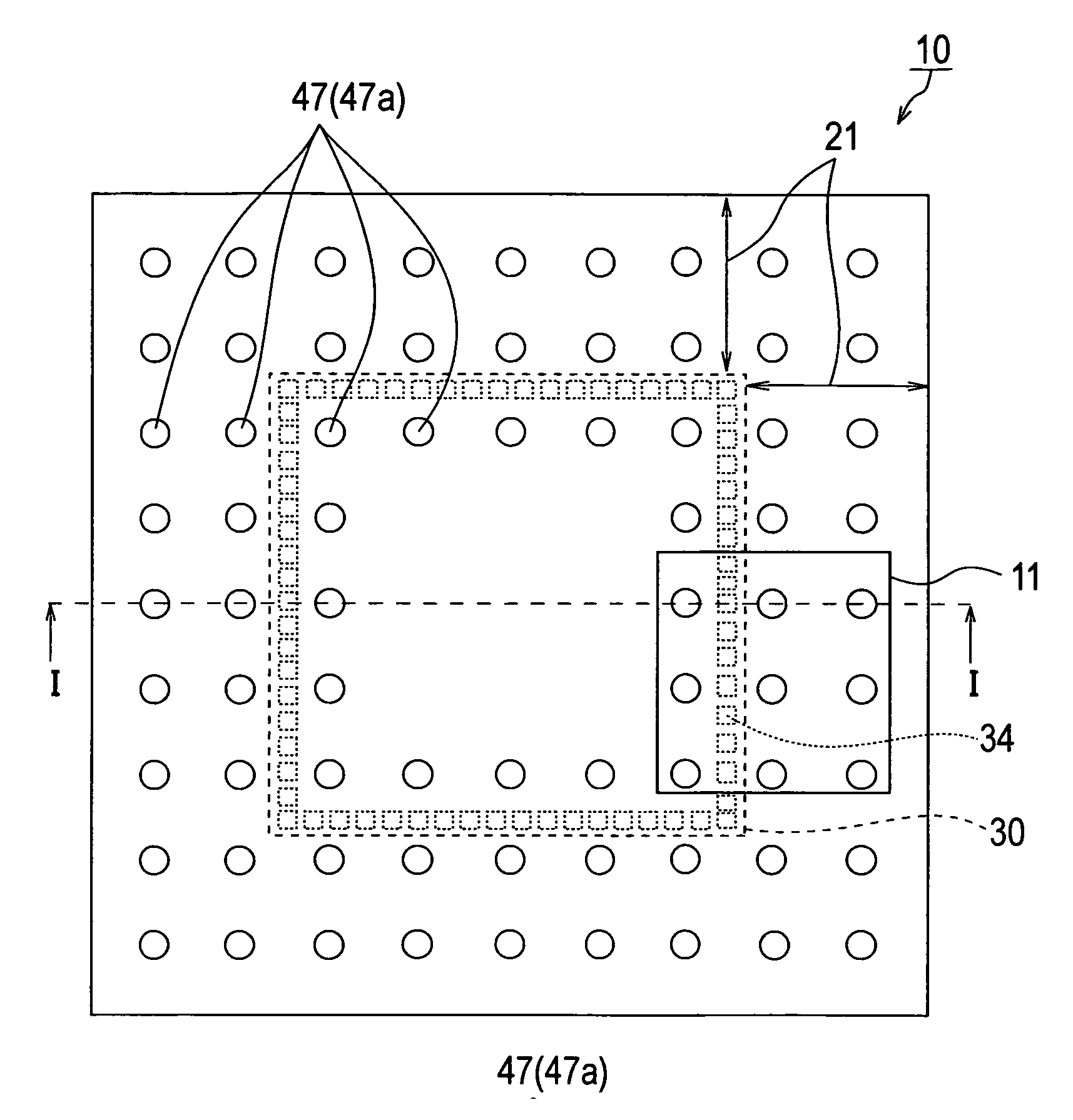
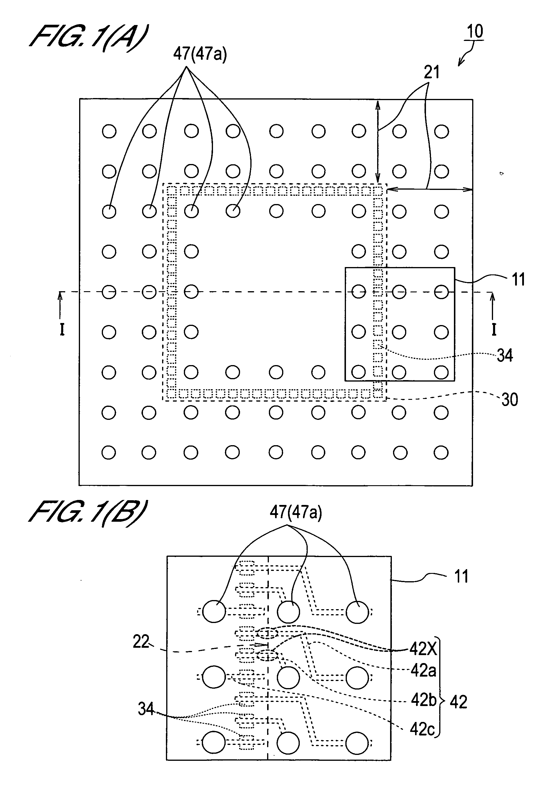
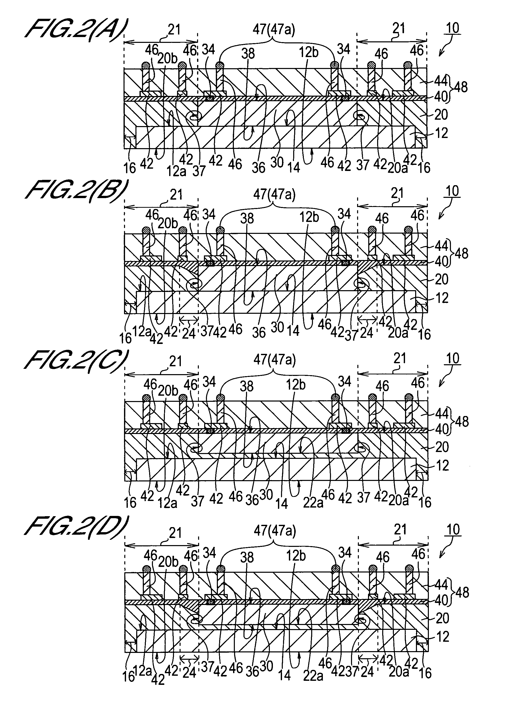
[0116] A constitutional example of a semiconductor device of this invention will be described with reference to FIGS. 1 and 2. FIG. 1(A) is a plan view ...


PUM


Abstract

A semiconductor device comprises: a semiconductor chip having a firstmain surface, asecondmain surface, and a plurality of side surfaces; an extension portion which contacts and surrounds the side surfaces of the semiconductor chip; a base, which is capable of conducting heat generated by the semiconductor chip; an insulating film which is formed on the first face and the first main surface; a plurality of wiring patterns extended from electrode pads to the upper side of the first face of the extension portion; a sealing portion which is formed on the wiring patterns and insulating film; and a plurality of external terminals provided over the wiring patterns in a region including the upper side of the extension portion.

Description

BACKGROUND OF THE INVENTION [0001] 1. Field of the Invention [0002] This invention relates to a semiconductor device and a manufacturing method therefor, and more particularly to a semiconductor device having a constitution which is capable of corresponding to further increases in the number of external terminals and a manufacturing method therefor. [0003] 2. Description of Related Art [0004] Demands have been made in recent years for further reductions in the size and thickness of packaged semiconductor devices. In response to such demands, a packaging form known as a Wafer Level Chip Size Package (to be referred to simply as WCSP hereinafter), in which the external size of the packaging is substantially equal to the external size of the semiconductor chip, has been proposed. [0005] AWCSP comprises a semiconductor chip. The semiconductor chip comprises a circuit element having a predetermined function and a plurality of electrode pads electrically connected to each other on the cir...

Claims


Application Information

Patent Timeline
Patent Type & Authority Applications(United States)
IPC IPC(8): H04N5/335H01L23/12H01L23/31H01L23/433
CPCH01L23/3114H01L2924/014H01L23/4334H01L23/5389H01L24/24H01L24/82H01L24/97H01L2224/24226H01L2224/97H01L2924/01004H01L2924/01013H01L2924/01029H01L2924/01074H01L2924/01078H01L2924/01079H01L2924/01082H01L2924/15311H01L2924/30107H01L23/3135H01L2924/01033H01L2924/01019H01L2924/01006H01L2924/01005H01L2224/82H01L2924/12042H01L2924/15787H01L2924/181H01L2924/351H01L2924/00
Inventor SHIZUNO, YOSHINORI
Owner LAPIS SEMICON CO LTD
Why Eureka
Try Eureka