Semi-transmissive liquid crystal display panel

Inactive Publication Date: 2007-03-29
JAPAN DISPLAY WEST
View PDF6 Cites 24 Cited by
  • Summary
  • Abstract
  • Description
  • Claims
  • Application Information

AI Technical Summary

Benefits of technology

[0042] Incidentally, in an MVA semi-transmissive liquid crystal display panel, when no electric field is applied, even when a pixel electrode does not overlap scan and signal lines in a transmissive portion, as seen in a plan view, there is no possibility of light leakage. However, a voltage applied to the scan line varies greatly, affecting the liquid crystal molecules. This may cause disturbance in the alignment of the liquid crystal molecules in the transmissi

Problems solved by technology

Disadvantageously, the backlight consumes a large amount of electric power.
The problem here is that this reflective liquid crystal display device uses external light as its light source, and hence suffers from poor visibility in a poorly-lit room, for example.
Now, since, for example, the users of mobile devices typified by mobile phones or the like are limited, there has conventionally not been so much demand to use a liquid crystal display panel having a wide viewing angle in small display portions of such mobile devices.
The problem here is

Method used


Image

  • Semi-transmissive liquid crystal display panel
  • Semi-transmissive liquid crystal display panel
  • Semi-transmissive liquid crystal display panel

Examples


Embodiment Construction

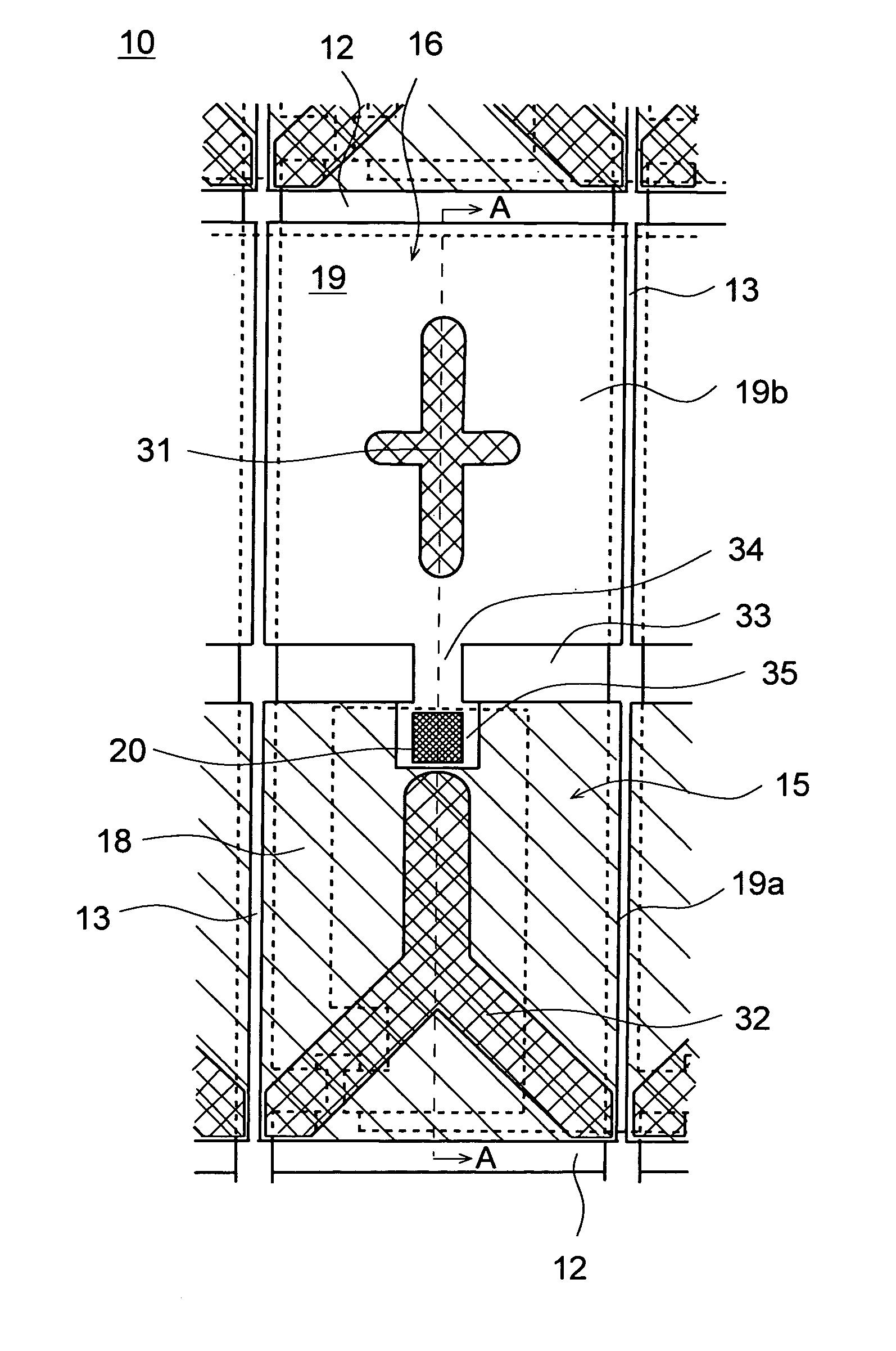
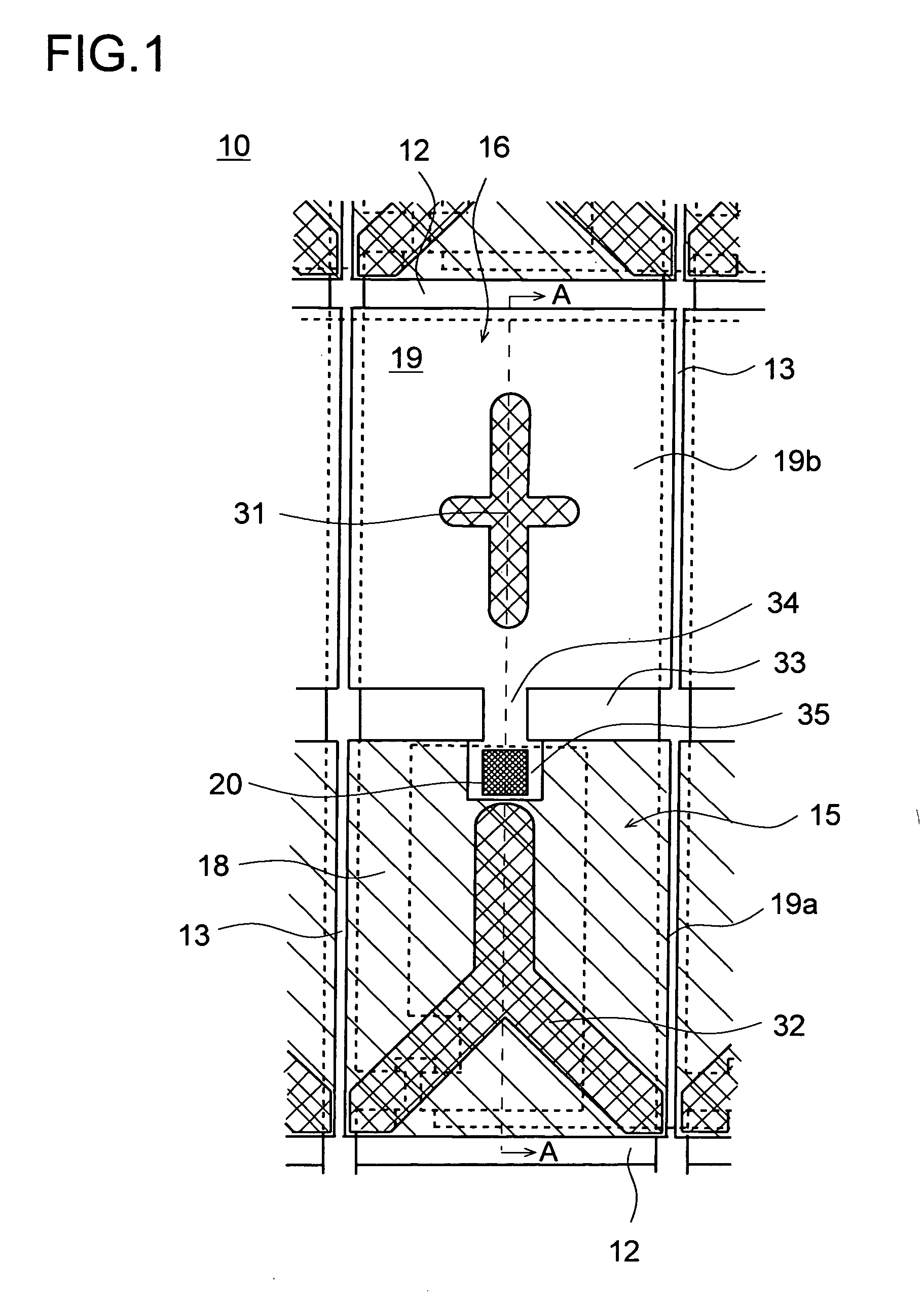
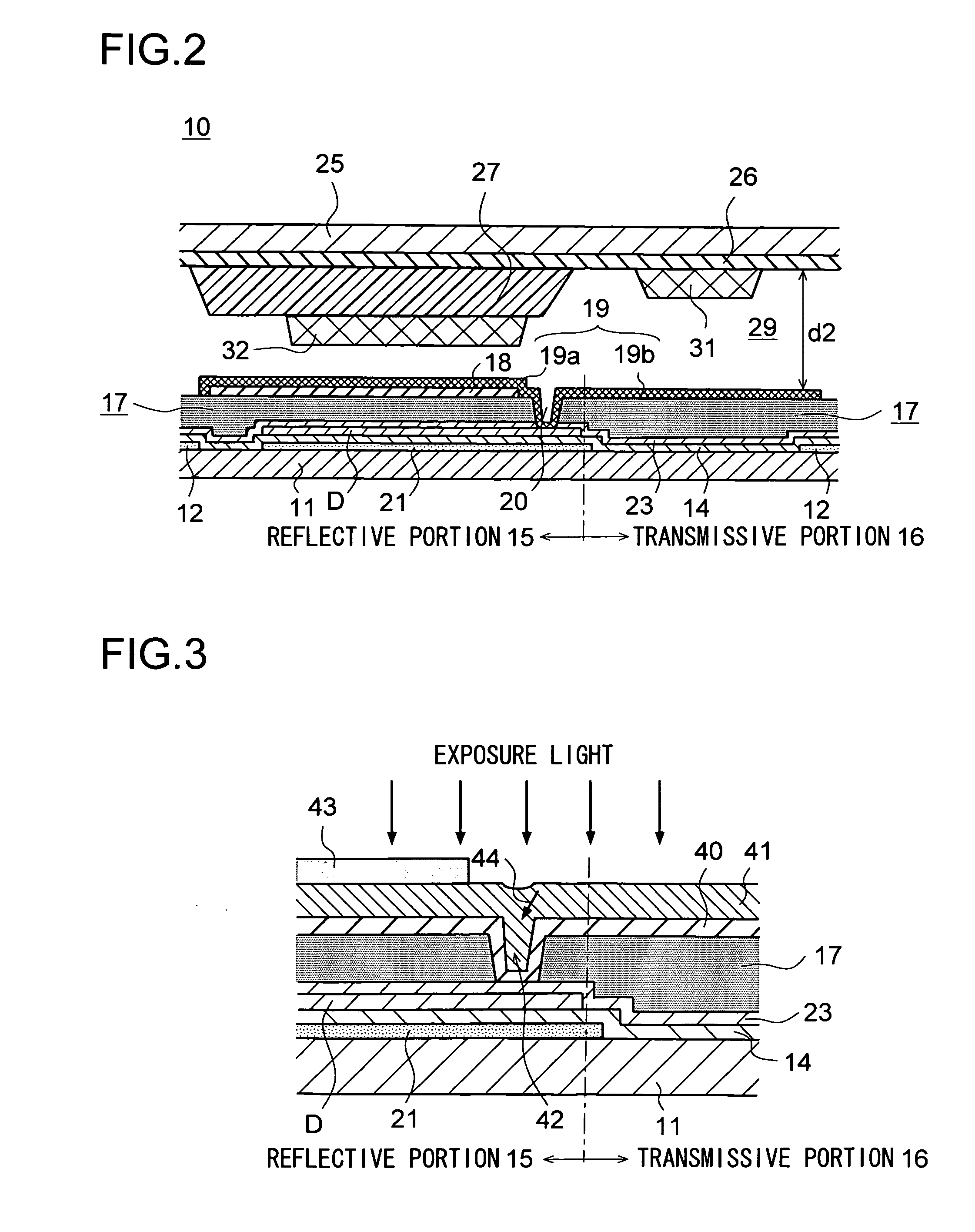
[0053] Hereinafter, embodiments of the present invention will be described specifically with reference to the accompanying drawings. It should be understood, however, that the embodiments presented below are simply intended to give an example of a semi-transmissive liquid crystal display panel that embodies the technical idea of the present invention, and therefore the semi-transmissive liquid crystal display panel specifically described below is not intended to limit in any way the manner in which to carry out the present invention. That is, the present invention finds wide application in the technical fields to which the appended claims are directed.

[0054] An MVA semi-transmissive liquid crystal display panel 10 embodying the present invention will be described with reference to FIGS. 1 to 3. FIG. 1 is a plan view showing one pixel of the MVA semi-transmissive liquid crystal display panel 10, as seen through the second substrate. FIG. 2 is a sectional view taken along line A-A sh...


PUM


Abstract

An semi-transmissive liquid crystal display panel is provided with a first substrate divided into sections by signal lines and scan lines arranged so as to form a matrix, each section having a switching element and a pixel electrode, the pixel electrode having transmissive and reflective portions. Here, at least the reflective portion of the first substrate has an interlayer film formed therein for separating the pixel electrode and the switching element, and a reflecting layer located below the pixel electrode, the reflecting layer has a notch portion at the edge thereof, and the pixel electrode formed in the reflective portion is electrically connected to an electrode of the switching element via a contact hole that is formed through the interlayer film in a part thereof corresponding to the notch portion.

Description

[0001] This application is based on Japanese Patent Application No. 2005-277245 filed on Sep. 26, 2005, the contents of which are hereby incorporated by reference. BACKGROUND OF THE INVENTION [0002] 1. Field of the Invention [0003] The present invention relates to a semi-transmissive liquid crystal display panel, and more particularly to a semi-transmissive liquid crystal display panel that can reduce contact hole formation time and thus offer a satisfactory production efficiency. [0004] 2. Description of Related Art [0005] In recent years, it has been becoming increasingly popular to use liquid crystal display devices not only in information communication devices but also in commonly used electric devices. A liquid crystal display device itself does not emit light, and hence a transmissive liquid crystal display device provided with a backlight is widely used. Disadvantageously, the backlight consumes a large amount of electric power. It is for this reason that, to reduce the elect...

Claims


Application Information

Patent Timeline
IPC IPC(8): G02F1/1335
CPCG02F1/133555G02F1/136227G02F1/133707
Inventor YOSHIDA, KOJITANAKA, SHINICHIRO
Owner JAPAN DISPLAY WEST
Why Eureka
Try Eureka