

Wafer level image module
a technology of image module and beam, applied in the field of beam level image module, can solve problems such as out-of-focus, and achieve the effect of improving image mapping quality
- Summary
- Abstract
- Description
- Claims
- Application Information
AI Technical Summary
Benefits of technology
Problems solved by technology
Method used
Image

Examples
Embodiment Construction
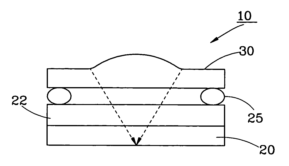
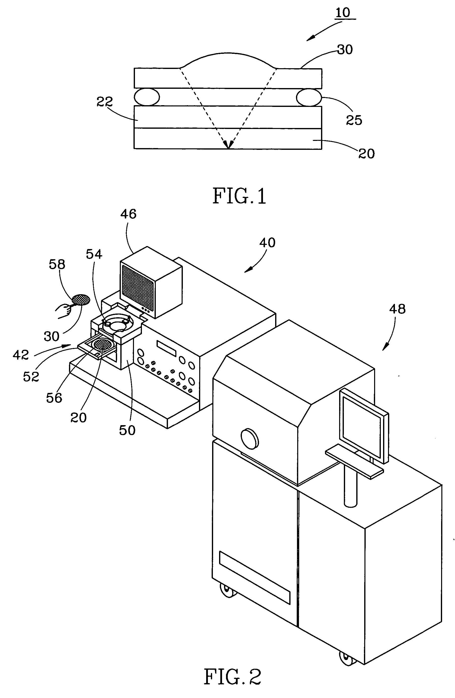
[0027] As shown in FIG. 1, a wafer level image module 10 in accordance with a first preferred embodiment of the present invention comprises a photo sensor 20, an adjustment member 25, and a lens set 30. The photo sensor 20 can be a CMOS (Complementary Metal-Oxide Semiconductor) image sensor or CCD (Charge Coupled Device) image sensor adapted to output an electrical signal when induced by light. The photo sensor 20 is mounted on the top side thereof with a light transmissive spacer 22. The light transmissive spacer 22 protects the photo sensor 20 against outside pollutants and moisture. The adjustment member 25 can be a glass ball spacer 25 or fiber spacer formed on the top surface of the transmissive spacer 22 by sputtering deposition, spot adhesive, or screen printing. The adjustment member 25 has a thickness about 1-50 μg m. This thickness is determined subject to the depth of focus required and the focus offset. Further, the adjustment member 25 can be formed on the transmissive ...
PUM
 Abstract
Description
Claims
Application Information