

Pulse modulation circuitry
a pulsed signal and circuit technology, applied in the direction of modulation, modulation, electromagnetic wave demodulation, etc., can solve the problems of small output power at the time of off state, and the ratio of pulsed signal output power
- Summary
- Abstract
- Description
- Claims
- Application Information
AI Technical Summary
Benefits of technology
Problems solved by technology
Method used
Image

Examples
embodiment 1
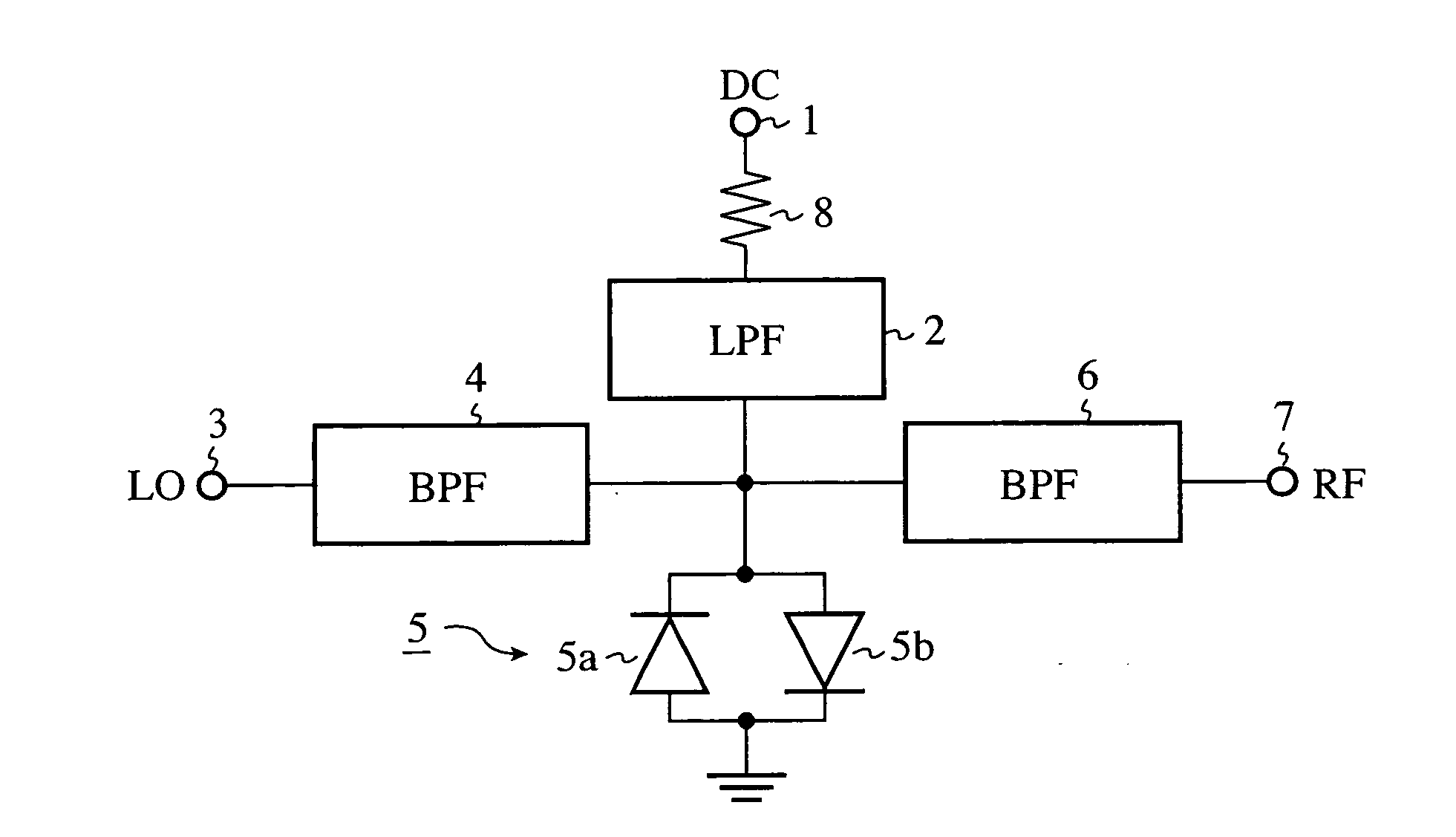
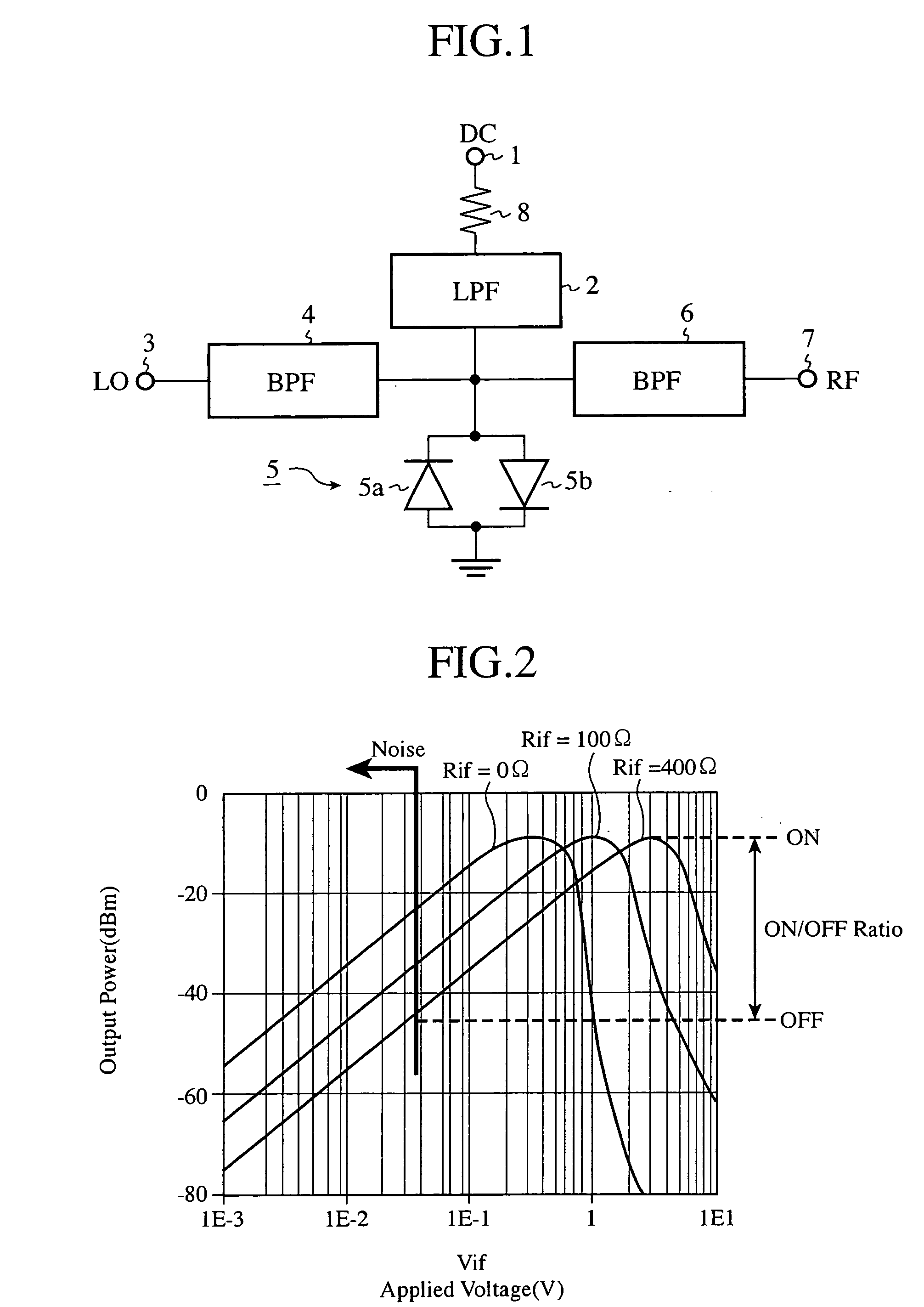
[0020]FIG. 1 is a block diagram showing pulse modulation circuitry in accordance with embodiment 1 of the present invention. In the figure, a low pass filter (referred to as an LPF from here on) 2 receives a DC pulsed signal (a pulsed signal) applied to a DC pulse applying terminal 1, removes an unnecessary wave component from the DC pulsed signal, and outputs a pulse component to an anti-parallel diode pair 5. A band pass filter (referred to as a BPF from here on) 4 receives a local oscillation signal LO applied to a local oscillation wave input terminal 3, removes an unnecessary wave component from the local oscillation signal LO, and outputs the local oscillation signal from which the unnecessary wave component is removed to the anti-parallel diode pair 5.
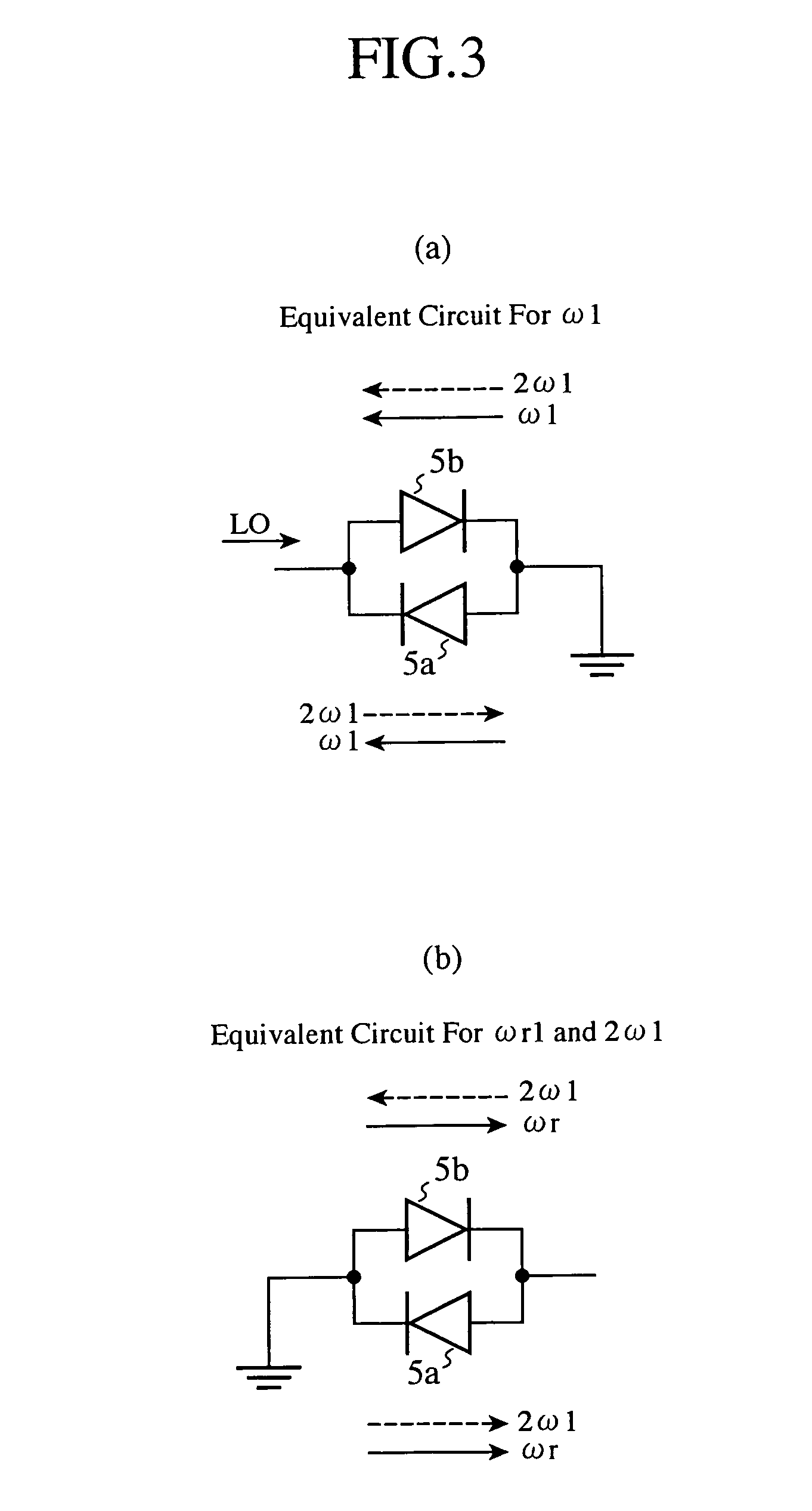
[0021] The anti-parallel diode pair 5 includes two diodes 5a and 5b which are connected in parallel with and opposite in direction to each other, and constitutes a mixing means for mixing the local oscillation signal LO from wh...
embodiment 2
[0043]FIG. 5 is a block diagram showing pulse modulation circuitry in accordance with embodiment 2 of the present invention. In the figure, since the same reference numerals as shown in FIG. 1 denote the same components as those of embodiment 1 or like components, the explanation of the components will be omitted hereafter.
[0044] A parallel circuit including a resistor 10 and a capacitor 11 constitutes a voltage dividing means, and is installed between an anti-parallel diode pair 5 and a ground.
[0045] Next, the operation of the pulse modulation circuitry in accordance with this embodiment of the present invention will be explained.
[0046] The pulse modulation circuitry in accordance with above-mentioned embodiment 1 includes the resistor 8 for dividing the voltage applied to the anti-parallel diode pair as previously mentioned. In contrast, in accordance with this embodiment, the resistor 10 of the parallel circuit can divide the voltage applied to the anti-parallel diode pair 5. ...
embodiment 3
[0048] In accordance with above-mentioned embodiment 2, the parallel circuit which consists of the resistor 10 and capacitor 11 is disposed between the anti-parallel diode pair 5 and the ground, as previously mentioned. In contrast, in accordance with this embodiment, a parallel circuit which consists of a resistor 10 and a capacitor 11 is disposed between a connecting point at which BPFs 4 and 6 are connected to each other, and an anti-parallel diode pair 5, as shown in FIG. 6. Therefore, this embodiment can provide the same advantages as offered by above-mentioned embodiment 2.
PUM
 Abstract
Description
Claims
Application Information