Dense OPC

a technology of opc and opc, applied in the field of optical and process correction, can solve the problems of inefficient and time-consuming process of estimating how features will print, optical distortion can occur,

Active Publication Date: 2007-03-29
SIEMENS PROD LIFECYCLE MANAGEMENT SOFTWARE INC
View PDF35 Cites 48 Cited by
  • Summary
  • Abstract
  • Description
  • Claims
  • Application Information

AI Technical Summary

Problems solved by technology

As the features on a mask become smaller and smaller, optical distortions can occur whereby the exposure pattern on a wafer will not match the pattern of features on the mask.
The simulations may overlap in some areas but be absent in other areas, thereby resulting in an inefficient and time consuming process of estimating how the features will print.

Method used


Image

  • Dense OPC
  • Dense OPC
  • Dense OPC

Examples


Embodiment Construction

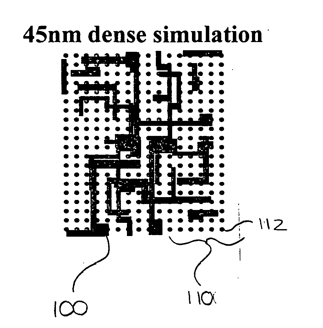
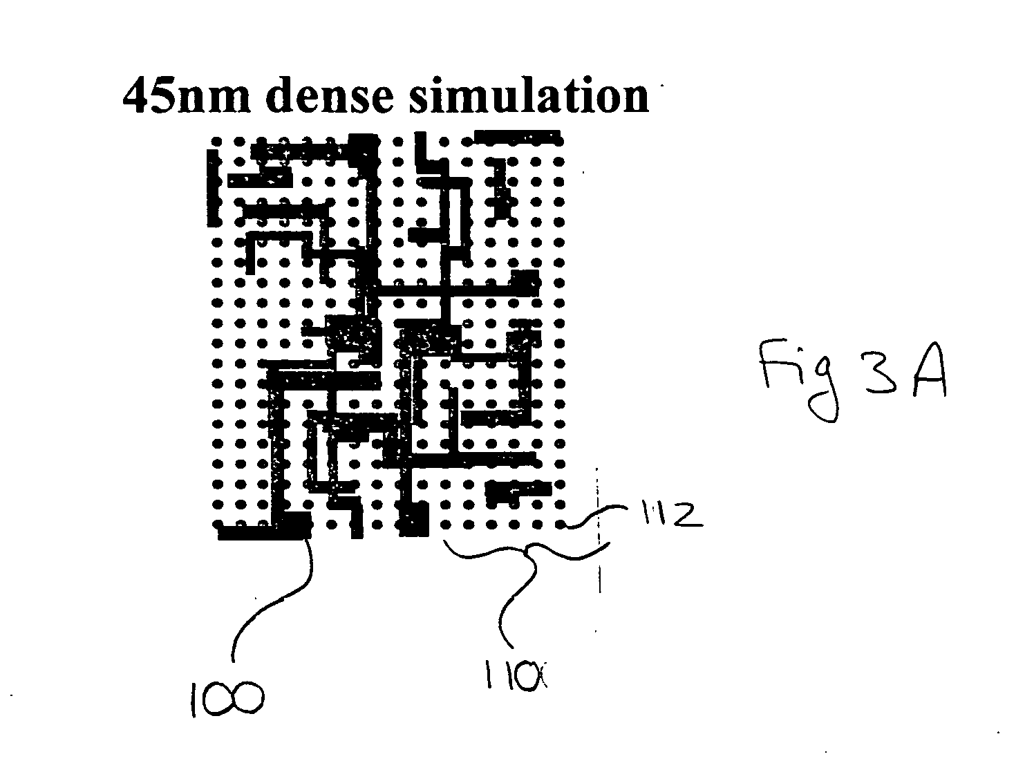
[0023] The present invention is a technique for calculating process conditions in order to perform optical and process correction (OPC) or other resolution enhancement techniques on a target layout design of features to be created on a semiconductor wafer.

[0024] As shown in FIG. 3A, a target layout design includes a number of features 100 that correspond to circuit elements to be created on a semiconductor wafer. In one embodiment, each feature 100 is defined as a polygon in a standard layout database language such as GDS-II or OASIS™. In order to improve the fidelity by which the pattern of features 100 can be created on a semiconductor wafer, simulations of one or more process conditions are performed on a grid 110 of sample points 112. The grid 110 may be uniform across the entire layout. Alternatively, the grid may have sample points 112 at a wider pitch in areas of the circuit contain fewer features or features that are not critical to circuit operation. Alternatively, those f...


PUM

PropertyMeasurementUnit
angleaaaaaaaaaa
anglesaaaaaaaaaa
areaaaaaaaaaaa

Abstract

A method of calculating process conditions for performing optical and process correction (OPC) or other resolution enhancement techniques on a layout design. Process conditions are estimated on a layout database on a substantially uniform grid. Contour curves are created from the estimated process conditions. The contour curves are then compared against the features in the layout to determine edge placement errors. From the edge placement errors, OPC or other corrections for the features can be made.

Description

FIELD OF THE INVENTION [0001] The present invention relates to photolithographic processing and, in particular, to optical and process correction. BACKGROUND OF THE INVENTION [0002] In conventional photolithographic processing, integrated circuits are created on a semiconductor wafer by exposing the wafer with a pattern of features printed on a mask or reticle. The pattern of features selectively exposes photosensitive chemicals on the wafer that is then further chemically and mechanically processed to build up layers of the integrated circuit. [0003] As the features on a mask become smaller and smaller, optical distortions can occur whereby the exposure pattern on a wafer will not match the pattern of features on the mask. To correct this, numerous resolution enhancement techniques such as the addition of subresolution assist features, phase shift masks, and optical and process correction (OPC) may be employed to improve the image fidelity so that the pattern imaged on a wafer more...

Claims


Application Information

Patent Timeline
Patent Type & Authority Applications(United States)
IPC IPC(8): G06F17/50G03F1/00G21K5/00G06F19/00
CPCG03F1/144G03F7/705G03F7/70441G03F1/36
Inventor BAILEY COBB, NICOLASDUDAU, DRAGOS
Owner SIEMENS PROD LIFECYCLE MANAGEMENT SOFTWARE INC
Why Eureka
Try Eureka