This helps you quickly interpret patents by identifying the three key elements:
Problems solved by technology
Method used
Benefits of technology
Benefits of technology
[0009] In view of this, it is an object of the invention to accomplish the aforementioned task in a display device equipped with a light-emitting element, so that the color reproduction area can be improved and the color gamut which can be viewed by human eyes can be widened.
Problems solved by technology
However, there is still a surplus in a color gamut which can be viewed by human eyes, and thus, a color reproduction area of a display device so far is still insufficient. FIG. 39 shows the CIE-XY chromaticity diagram which is established by COMMISSION INTERNATIONALE DE L'ECLAIRAGE (INTERNATIONAL COMMISSION ON ILLUMINATION: CIE) managing standards of color internationally.
Method used
Image
Click on the blue label to locate the original text in one second.
Reading with bidirectional positioning of images and text.
Examples
embodiment mode 1
[Configuration of a Display Device in this Embodiment Mode]
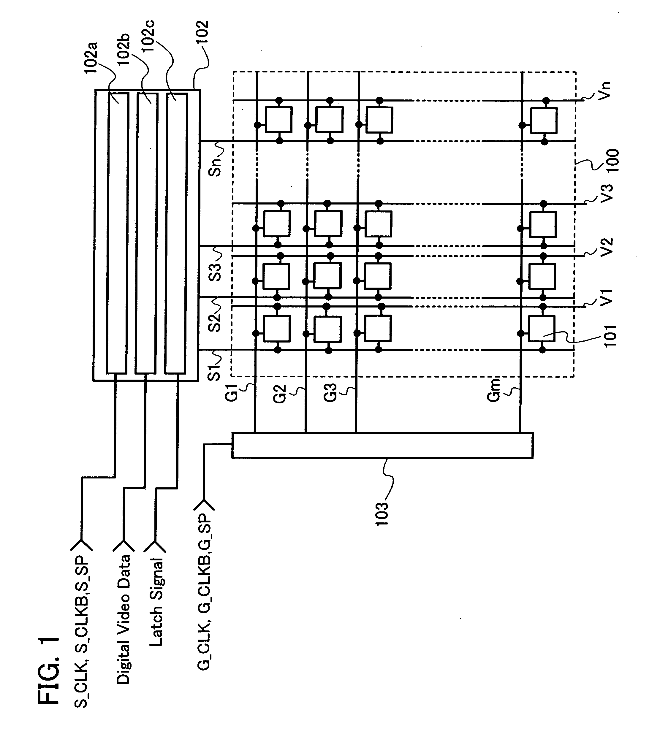
[0113] A configuration example of a display device in the invention is shown by a block diagram in FIG. 1. Reference numeral 100 denotes a pixel portion where a plurality of pixels 101 are arranged in matrix, and such a configuration is called an active matrix arrangement. In addition, reference numeral 102 denotes a signalline driver circuit and 103 denotes a scan linedriver circuit.
[0114] Note that the signalline driver circuit 102 and the scan linedriver circuit 103 are formed over the same substrate as a pixel portion 100 in FIG. 1; however, the configuration of the invention is not limited to this. The signalline driver circuit 102 and the scan linedriver circuit 103 may be formed over a different substrate from the pixel portion 100, and connected to the pixel portion 100 with a connector such as a flexible printed circuit (FPC). As a method for mounting the FPC, a connecting method using an anisotropic conduct...
embodiment mode 2
[0198] In this embodiment mode, a different configuration of light-emitting elements from the configuration of the light-emitting elements in the display of the invention in the aforementioned embodiment mode is described.
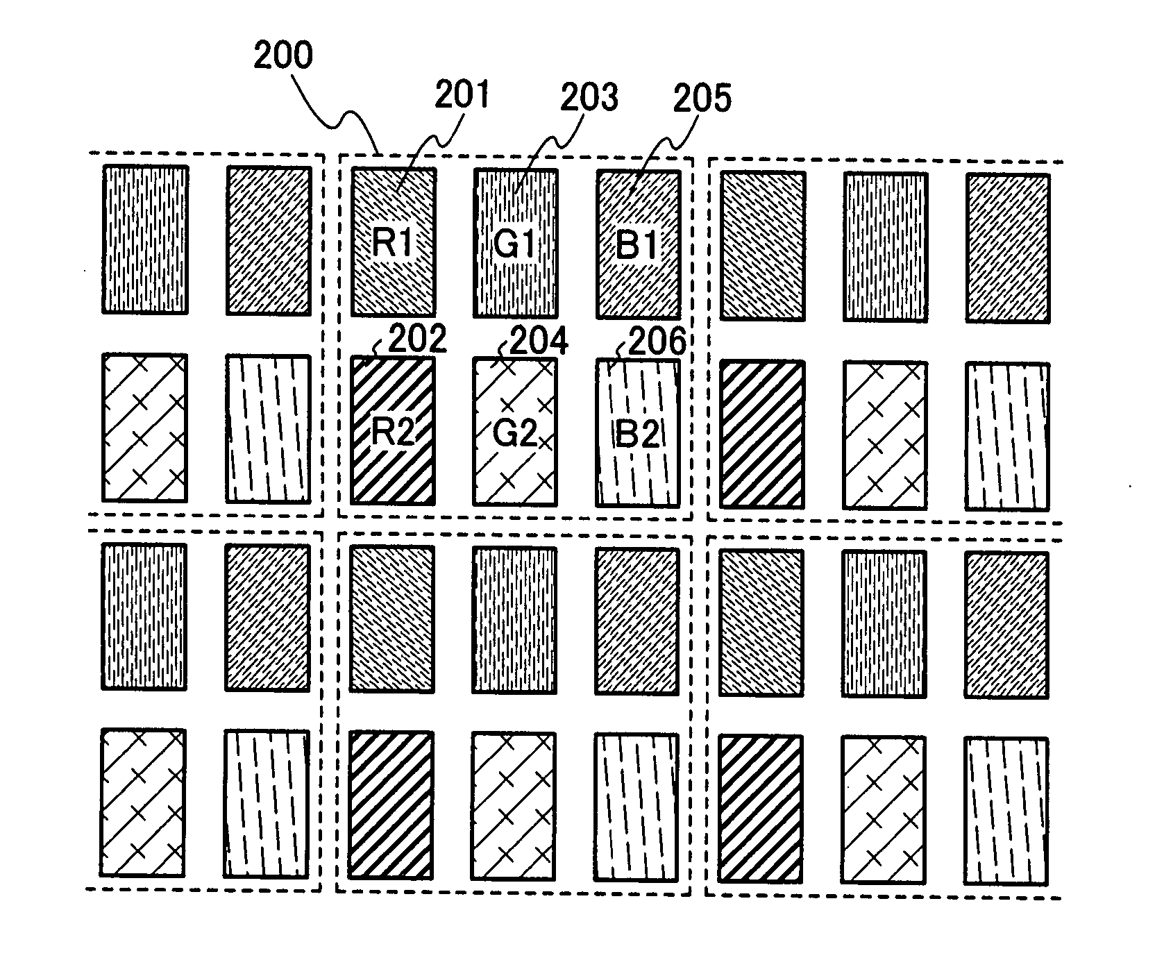
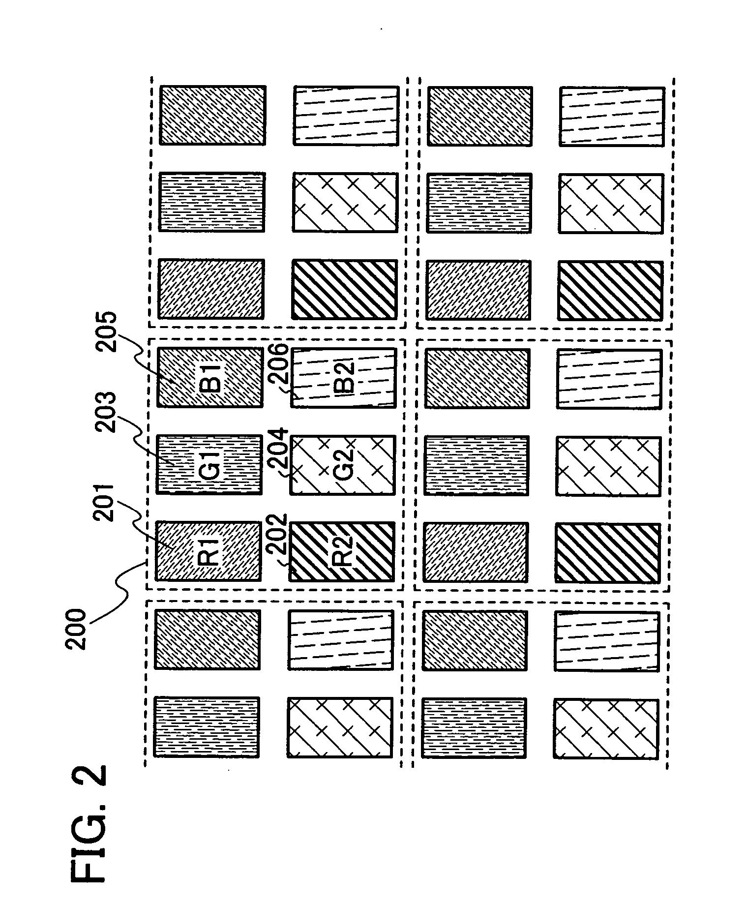
[0199] Description has been made of the configuration of the pixel portion of the invention with reference to FIG. 2 where the picture element of the invention includes the first pixel, the second pixel, the third pixel, the fourth pixel, the fifth pixel, and the sixth pixel. In addition, a light-emitting element is provided in each of the first pixel to the sixth pixel, so that a light-emitting element R1, a light-emitting element R2, a light-emitting element G1, a light-emitting element G2, a light-emitting element B1, and a light-emitting element B2 are connected to the first pixel, the second pixel, the third pixel, the fourth pixel, the fifth pixel, and the sixth pixel, respectively.
[0200] In this specification, the light-emitting element R1 in the first pix...
embodiment mode 3
[0216] In this embodiment mode, a different configuration of light-emitting elements from the configuration of the light-emitting elements in the display of the invention in the aforementioned embodiment modes is described.
[0217] Description has been made of the configuration of the pixel portion of the invention where the picture element of the invention includes the first pixel, the second pixel, the third pixel, the fourth pixel, the fifth pixel, and the sixth pixel in FIG. 2 In addition, a light-emitting element is provided in each of the first pixel to the sixth pixel, such that a light-emitting element R1, a light-emitting element R2, a light-emitting element G1, a light-emitting element G2, a light-emitting element B1, and a light-emitting element B2 are connected to the first pixel, the second pixel, the third pixel, the fourth pixel, the fifth pixel, and the sixth pixel, respectively.
[0218] In this specification, the light-emitting element R1 of the first pixel and the li...
PUM
Abstract
To improve color reproduction areas in a display device having light-emitting elements. A display region has a plurality of picture elements. Each picture element includes: first and second pixels each including a light-emitting element which has a chromaticity whose x-coordinate in a CIE-XY chromaticity diagram is 0.50 or more; third and fourth pixels each including a light-emitting element which has a chromaticity whose y-coordinate in the diagram is 0.55 or more; and fifth and sixth pixels each including a light-emitting element which has a chromaticity whose x-coordinate and y-coordinate in the diagram are 0.20 or less and 0.25 or less, respectively. The light-emitting elements in the first and second pixels have different emission spectrums from each other; the light-emitting elements in the third and fourth pixels have different emission spectrums from each other; and the light-emitting elements in the fifth and sixth pixels have different emission spectrums from each other.
Description
BACKGROUND OF THE INVENTION [0001] 1. Field of the Invention [0002] The present invention relates to a display device equipped with a light-emitting element or an electro-optical element in a pixel. In particular, the present invention relates to a display device having a layer including an organic material, a fluorescent material, or a phosphorescent material in the light-emitting element. [0003] 2. Description of the Related Art [0004] A display device having a light-emitting element which includes a layer of an organic material between a pair of electrodes and emits light when a current is supplied between the electrodes has been developed. Such a display device has an advantage in reducing thickness and weight, has high visibility due to the self-luminance, and has high response speed. In addition, since power consumption of such a display device may potentially be made very small, it has been actively developed as a device of next generation, and some of such devices have been ...
Claims
Application Information
Patent Timeline
Application Date:The date an application was filed.
Publication Date:The date a patent or application was officially published.
First Publication Date:The earliest publication date of a patent with the same application number.
Issue Date:Publication date of the patent grant document.
PCT Entry Date:The Entry date of PCT National Phase.
Estimated Expiry Date:The statutory expiry date of a patent right according to the Patent Law, and it is the longest term of protection that the patent right can achieve without the termination of the patent right due to other reasons(Term extension factor has been taken into account ).
Invalid Date:Actual expiry date is based on effective date or publication date of legal transaction data of invalid patent.

