Electro-optical device, driving method therefor, and electronic apparatus

a driving method and optical technology, applied in the direction of electric digital data processing, instruments, computing, etc., can solve the problem of wide voltage range, and achieve the effect of reducing the character requirements of switching elements of pixels and a circuit for driving scanning lines

Active Publication Date: 2007-04-05
SEIKO EPSON CORP
View PDF5 Cites 18 Cited by
  • Summary
  • Abstract
  • Description
  • Claims
  • Application Information

AI Technical Summary

Benefits of technology

[0007] An advantage of the invention is that it provides a technique for alternately applying high and low voltages to a common electrode, and more specifically, it provides an electro-optical device in which the voltage range required for switching elements of pixels and a circuit for driving scanning lines can be reduced, a driving method for the electro-optical device, and an electronic apparatus.
[0008] According to an aspect of the invention, an electro-optical device includes pixel electrodes corresponding to intersections of a plurality of scanning lines and a plurality of data lines and specific to the pixels, a common electrode facing the pixel electrode, and a switching element that establishes conduction between the data line and the pixel electrode when a selection voltage is applied to the scanning line, a control circuit that supplies a high voltage having a predetermined value and a low voltage lower than the high voltage alternately at predetermined intervals to the common electrode; a scanning line driving circuit that selects the plurality of scanning lines in a predetermined order and that applies the selection voltage to each of the selected scanning lines; and a data line driving circuit that supplies a data signal defining the grayscale levels of the pixels to the data lines in a period during which one of the scanning lines is selected and during which the voltage applied to the common electrode is maintained at the high voltage or the low voltage and that performs a precharge operation for precharging the plurality of data lines to a predetermined potential in a period of time including a period during which the voltage applied to the common electrode changes from one of the high voltage and the low voltage to the other. According to the aspect of the invention, the characteristic requirements for switching elements of pixels and a circuit for driving scanning lines can be reduced.
[0009] In this case, the precharge operation may begin and end in the period during which the voltage applied to the common electrode changes from the one of the high voltage and the low voltage to the other. Alternatively, the precharge operation may begin in the period during which the voltage applied to the common electrode changes from the one of the high voltage and the low voltage to the other, and the precharge operation may end in a period during which the voltage applied to the common electrode is maintained constant at the other of the high voltage and the low voltage. Still alternatively, the precharge operation may begin in a period in which the voltage applied to the common electrode is maintained constant at the one of the high voltage and the low voltage, and the precharge operation may end in the period during which the voltage applied to the common electrode changes from the one of the high voltage and the low voltage to the other.
[0010] In the electro-optical device, the precharge operation may begin and end in a period during which the selection voltage is applied to the scanning line.
[0011] The invention can be conceptualized as providing not only an electro-optical device but also a driving method for the electro-optical device and an electronic apparatus including the electro-optical device.

Problems solved by technology

Although the technique allows simplification of a circuit for driving data lines, there arises another problem in that a wider voltage range may be required for switching elements of pixels and a scanning line circuit for driving scanning lines.

Method used


Image

  • Electro-optical device, driving method therefor, and electronic apparatus
  • Electro-optical device, driving method therefor, and electronic apparatus
  • Electro-optical device, driving method therefor, and electronic apparatus

Examples


Embodiment Construction

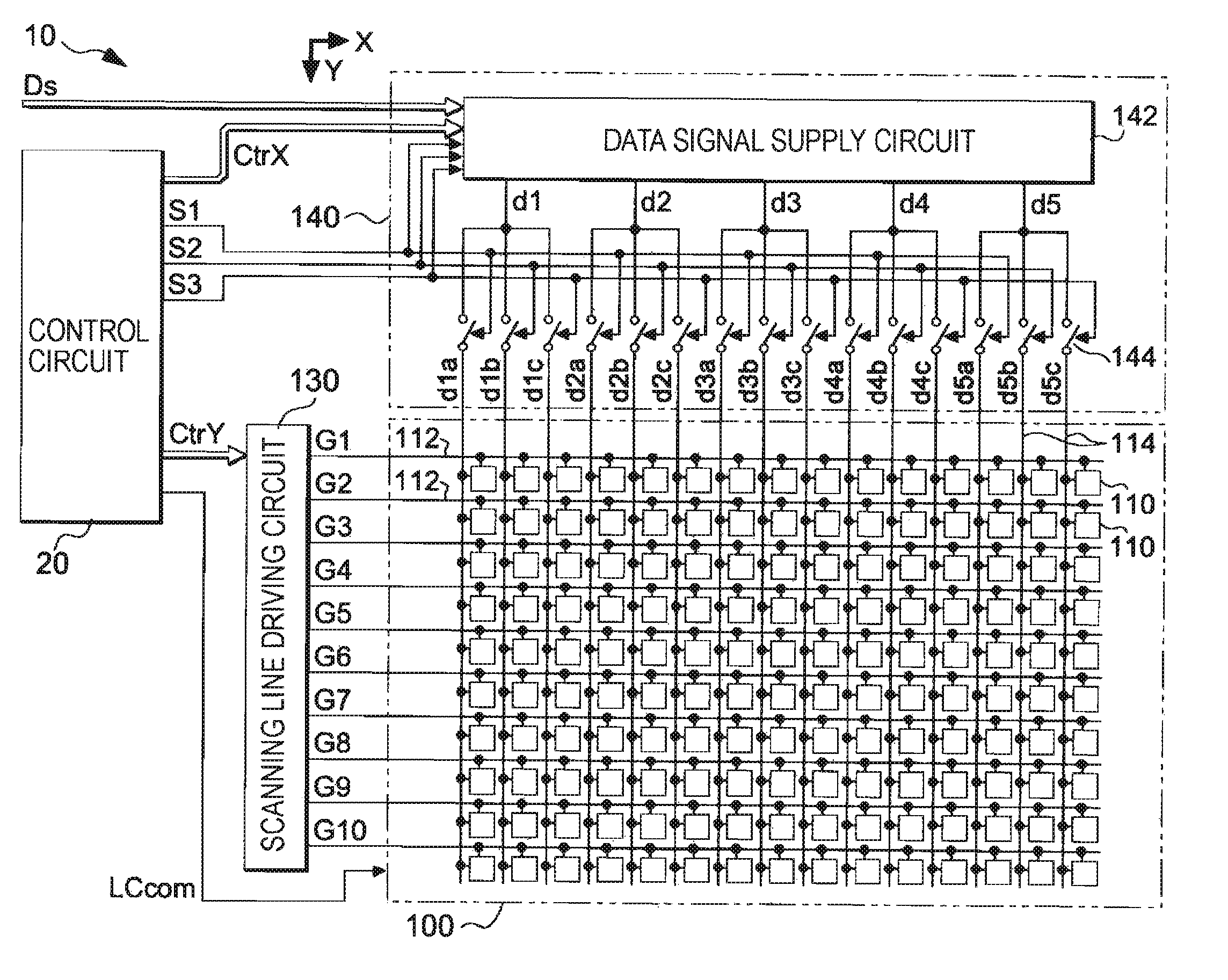
[0024] An embodiment of the invention will be described with reference to the drawings. FIG. 1 is a block diagram showing a structure of an electro-optical device 10 according to an embodiment of the invention.

[0025] As shown in FIG. 1, the electro-optical device 10 includes a control circuit 20, a display area 100, a scanning line driving circuit 130, and a data line driving circuit 140. In the display area 100, 10 scanning lines 112 arranged in rows extend in the row direction (X-direction), and 15 data lines 114 arranged in columns extend in the column direction (Y-direction).

[0026] Pixels 110 are placed at intersections of the LO scanning lines 112 and the 15 data lines 114. In the embodiment, therefore, the pixels 110 are arranged in a matrix of 10 vertical rows and 15 horizontal columns. However, it is to be understood that the invention is not limited to that arrangement.

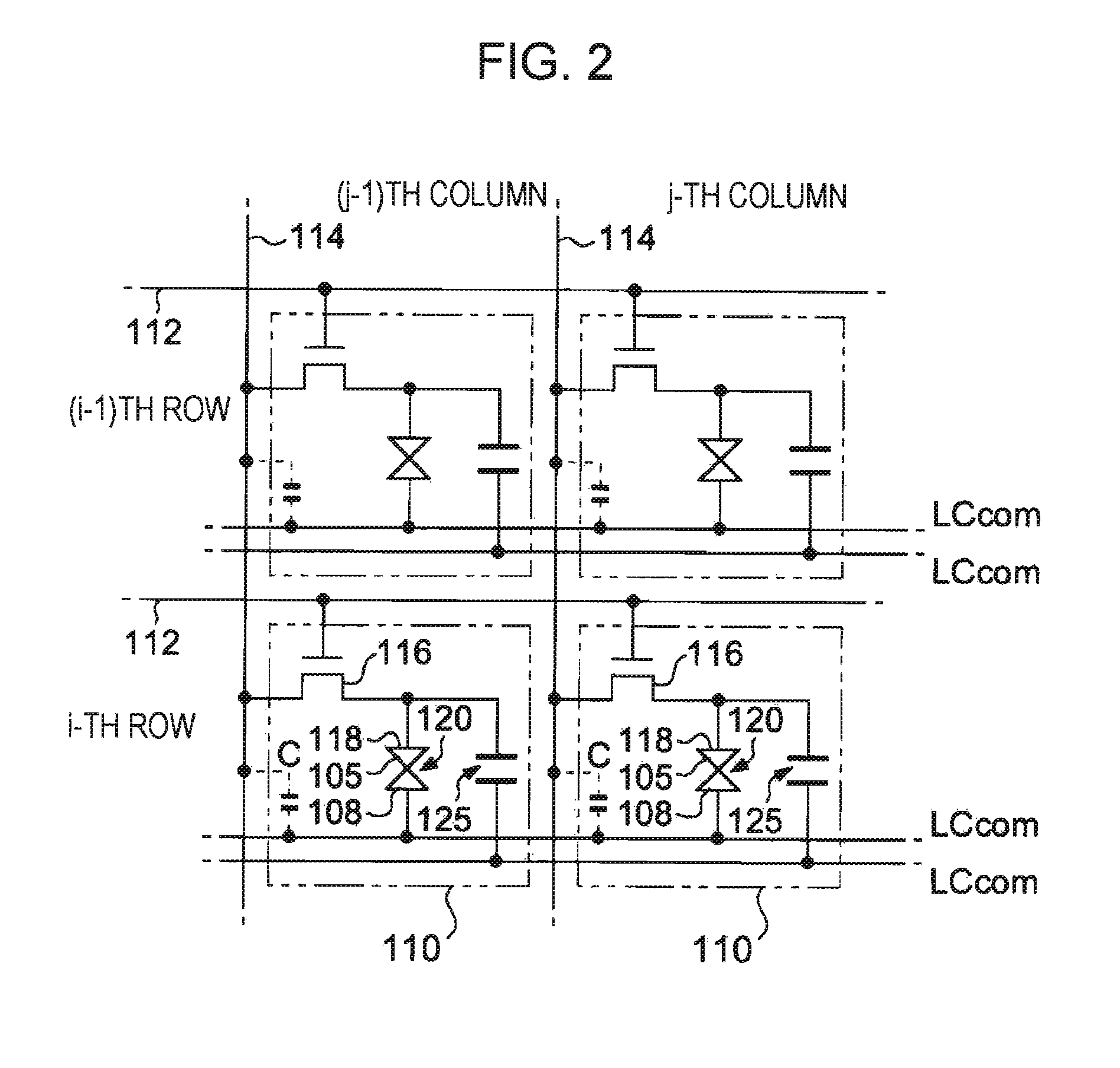
[0027] The structure of the pixels 110 will be described. FIG. 2 illustrates an electrical structure of...


PUM


Abstract

An electro-optical device includes pixel electrodes corresponding to intersections of a plurality of scanning lines and a plurality of data lines and specific to the pixels. A common electrode facing the pixel electrode, and A switching element that establishes conduction between the data line and the pixel electrode when a selection voltage is applied to the scanning line. A control circuit that supplies a high voltage having a predetermined value and a low voltage lower than the high voltage alternately at predetermined intervals to the common electrode; A scanning line driving circuit that selects the plurality of scanning lines in a predetermined order and that applies the selection voltage to each of the selected scanning lines; and A data line driving circuit that supplies a data signal defining the grayscale levels of the pixels to the data lines in a period during which one of the scanning lines is selected and during which the voltage applied to the common electrode is maintained at the high voltage or the low voltage and that performs a precharge operation for precharging the plurality of data lines to a predetermined potential in a period of time including a period during which the voltage applied to the common electrode changes from one of the high voltage and the low voltage to the other.

Description

BACKGROUND [0001] 1. Technical Field [0002] The present invention relates to techniques for simplifying the structure of electro-optical devices such as liquid crystal display devices. [0003] 2. Related Art [0004] In an electro-optical device for performing display using electro-optical changes, such as a liquid crystal device, pixels are provided at intersections of scanning lines (gate lines) and data lines (source lines) Each of the pixels generally includes a capacitor holding an electro-optical material, such as liquid crystal, between a pixel electrode and a common electrode having a constant potential, and a switching element that establishes conduction between the data line and the pixel electrode when the scanning line is selected. The grayscale level (or brightness) of each pixel is determined by an effective voltage value stored in the capacitor. In a case where liquid crystal is used as the electro-optical material, the pixels are basically alternating-current driven, an...

Claims


Application Information

Patent Timeline
Patent Type & Authority Applications(United States)
IPC IPC(8): G09G3/36
CPCG09G3/3614G09G3/3648G09G3/3688G09G2310/0248G09G2310/0297G09G2310/08G02F1/133G09G3/20G09G3/36
Inventor ITO, AKIHIKO
Owner SEIKO EPSON CORP
Why Eureka
Try Eureka