
Trimming circuit, electronic circuit, and trimming control system

a technology of electronic circuits and trimming control systems, applied in emergency protective devices, semiconductor/solid-state device details, instruments, etc., can solve problems such as assembly shift, change of band gap, and change of characteristics of semiconductor devices, so as to reduce the risk of failure and be easily manufactured through trimming

Inactive Publication Date: 2007-04-12
NXP USA INC
View PDF5 Cites 11 Cited by
  • Summary
  • Abstract
  • Description
  • Claims
  • Application Information

AI Technical Summary

Benefits of technology

The present invention provides a trimming circuit and control system that reduces the risk of failing to perform trimming and ensures that the desired device is readily manufactured through trimming. The trimming circuit includes a fuse, a probe pad for performing probe trimming, and a trimming selecting means for performing package trimming. The trimming control system includes a wafer tester, a package tester, and a trimming management data storing means for identifying a lot manufactured in a common process and locating a trimming circuit in the lot. The technical effects of the invention include improving the manufacturing process and reducing defective devices.

Problems solved by technology

However, the characteristics of a semiconductor device may change after packaging.
For example, the application of stress to a chip subsequent to molding may result in an assembly shift, which would change the band gap.
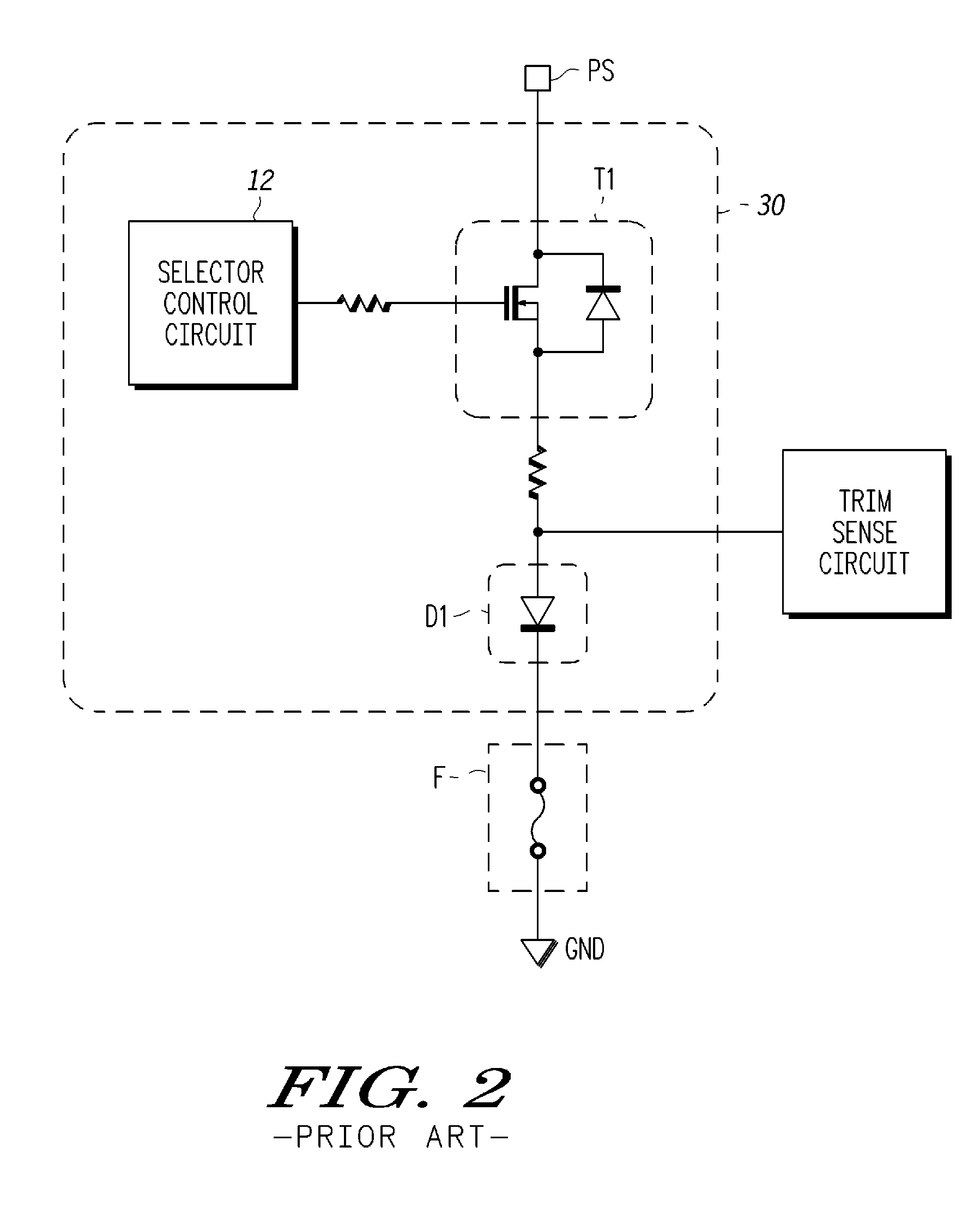
However, depending on the characteristics of the current supply circuit or the fuse (e.g., depending on variations of the fuse resistor), a sufficient amount of current may not be supplied.
In particular, package trimming has high process dependency.
Therefore, package trimming may fail to enable sufficient trimming when package trimming is performed on a device that is manufactured with new processes and includes a current supply circuit or fuses with varying characteristics.

Method used


Image

  • Trimming circuit, electronic circuit, and trimming control system
  • Trimming circuit, electronic circuit, and trimming control system
  • Trimming circuit, electronic circuit, and trimming control system

Examples


Embodiment Construction

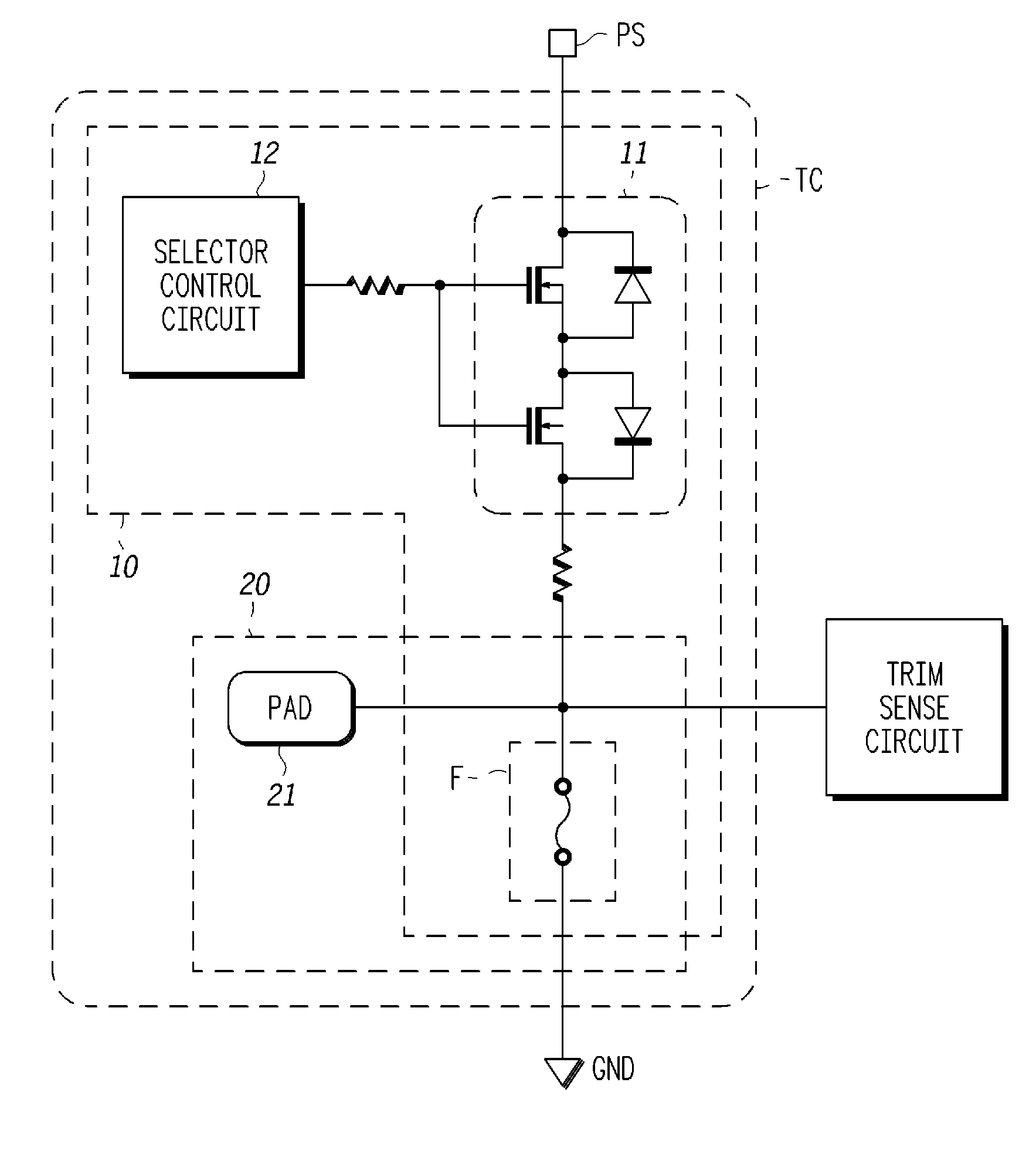
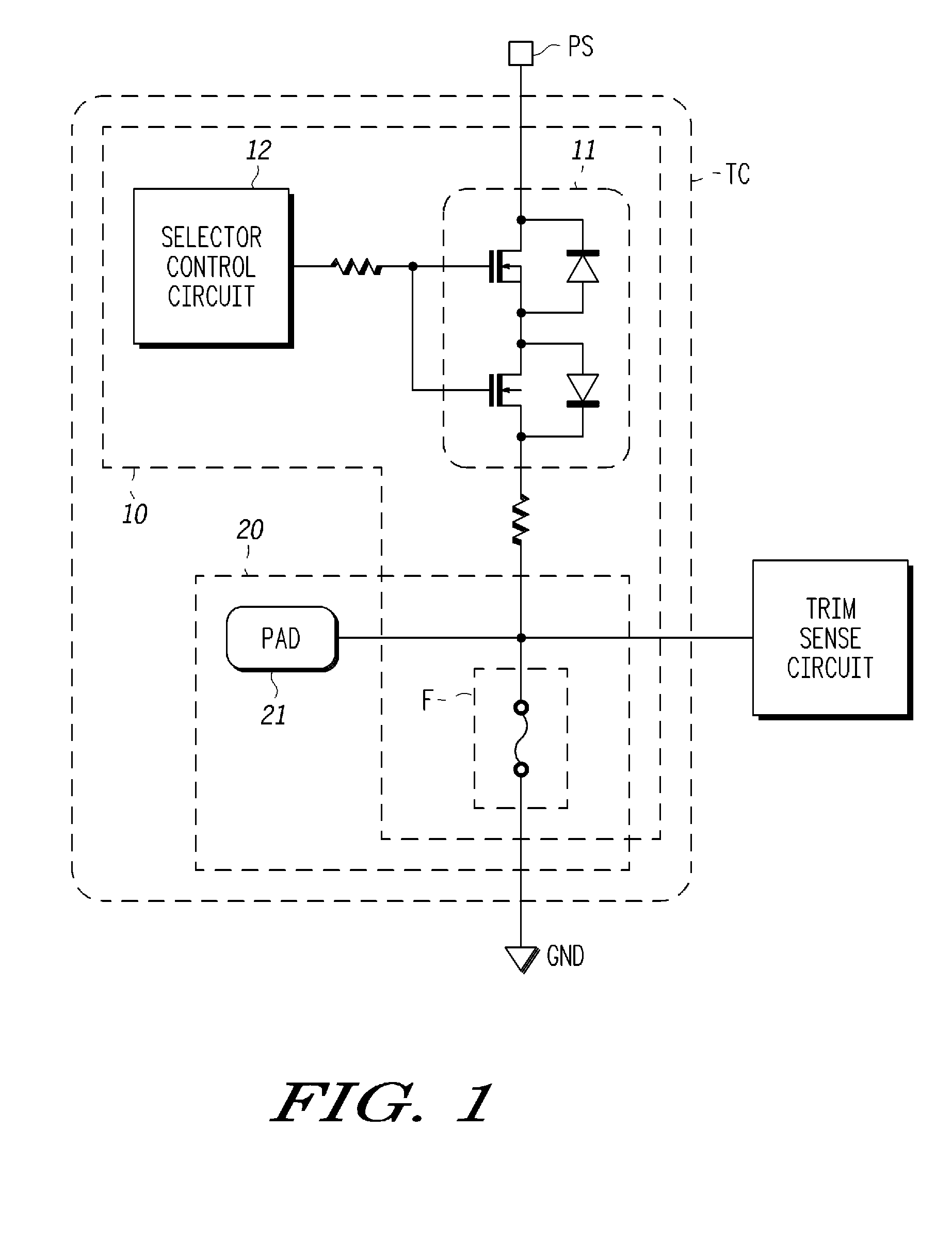
[0016] A trimming circuit according to a preferred embodiment of the present invention will now be described. The trimming circuit is applied to a reference voltage generation circuit of a semiconductor device. The reference voltage generation circuit includes a plurality of trimming circuits. A trim sense circuit is connected to each trimming circuit. FIG. 1 shows the basic structure of a trimming circuit TC in accordance with an embodiment of the present invention. The trimming circuit TC includes a selector 11, a resistor, and a fuse F, which are connected in series between a power supply PS and ground GND. A probe pad 21 for performing probe trimming is connected to a position immediately above the fuse F.

[0017] The selector 11 is formed by two n-type MOS transistors, which are back-to-back connected. Each n-type MOS transistor has a gate terminal, which functions as a control terminal and which is connected to a selector control circuit 12. The selector 11 and the selector con...


PUM


Abstract

A trimming circuit, an electronic circuit, and a trimming control system for reducing the risk of failures when perform trimming and for ensuring that a desired device is readily manufactured. A selector, a resistor, and a fuse are connected in series between a power supply and ground. A probe pad for performing probe trimming is connected immediately above the fuse. The selector includes two back-to-back connected n-type MOS transistors. Each n-type MOS transistor has a gate terminal connected to a selector control circuit. A trim sense circuit is arranged at a power supply side of the fuse. The trim sense circuit detects fuse breakage and changes the operation of an element associated with each trimming circuit TC based on the detection.

Description

BACKGROUND OF THE INVENTION [0001] The present invention relates to a trimming circuit, an electronic circuit, and a trimming control system for an electronic circuit, such as a semiconductor device, for adjusting electrical characteristics of the electronic circuit. [0002] In a semiconductor integrated circuit, a fuse may be used to realize a desired operation setting or a desired adjustment. For example, an electronic circuit, such as a semiconductor device, may use a trimming circuit to adjust the characteristics of the electronic circuit. The trimming circuit changes the resistance through the switch operation of a transistor and includes a fuse circuit for performing such a switching operation. The fuse circuit has a plurality of fuses and controls the switch operation of a trim sense circuit corresponding to each fuse by breaking or not breaking each fuse. [0003] When trimming is executed, “probe trimming” is often performed in the prior art (refer to, for example, Japanese La...

Claims


Application Information

Patent Timeline
Patent Type & Authority Applications(United States)
IPC IPC(8): H01H37/76
CPCH01L23/5256H01L2924/0002H01L2924/00
Inventor TAKI, KONOSUKEFUKAZAWA, HIDETAKA
Owner NXP USA INC
Learn More