Assembly process for out-of-plane MEMS and three-axis sensors

a three-axis sensor and out-of-plane technology, applied in the direction of microstructural device assembly, acceleration measurement using interia forces, instruments, etc., can solve the problems of difficult to obtain macro-scale assembly, difficult to perfectly align the three different sensors perpendicularly, etc., and achieve the effect of more robust structur

Inactive Publication Date: 2007-04-19
RGT UNIV OF CALIFORNIA
View PDF0 Cites 43 Cited by
  • Summary
  • Abstract
  • Description
  • Claims
  • Application Information

AI Technical Summary

Benefits of technology

[0007] In the method of the illustrated embodiment of the invention, a sensor or accelerometer fabricated into an out-of-plane wafer or chip can be inserted into a cavity in a holder wafer, which in addition to holding the sensor in place also provides electrical conduction between the inserted sensor and the holder wafer or substrate. The use of SOI holder wafers allows for a more robust structure, since fingers for holding and contacting the out-of-plane wafer can be fabricated from the device layer in an SOI wafer, which fingers are much thicker than the very thin layer of silicon nitride or silicon carbide in the prior art assemblies.

Problems solved by technology

However, this method is only used for passive components.
However, it is very difficult to perfectly align the three different sensors perpendicularly when using this technique.
Also, all three sensors should ideally have the same center of gravity, which is very hard to obtain with macro-scale assembly.

Method used


Image

  • Assembly process for out-of-plane MEMS and three-axis sensors
  • Assembly process for out-of-plane MEMS and three-axis sensors
  • Assembly process for out-of-plane MEMS and three-axis sensors

Examples


Embodiment Construction

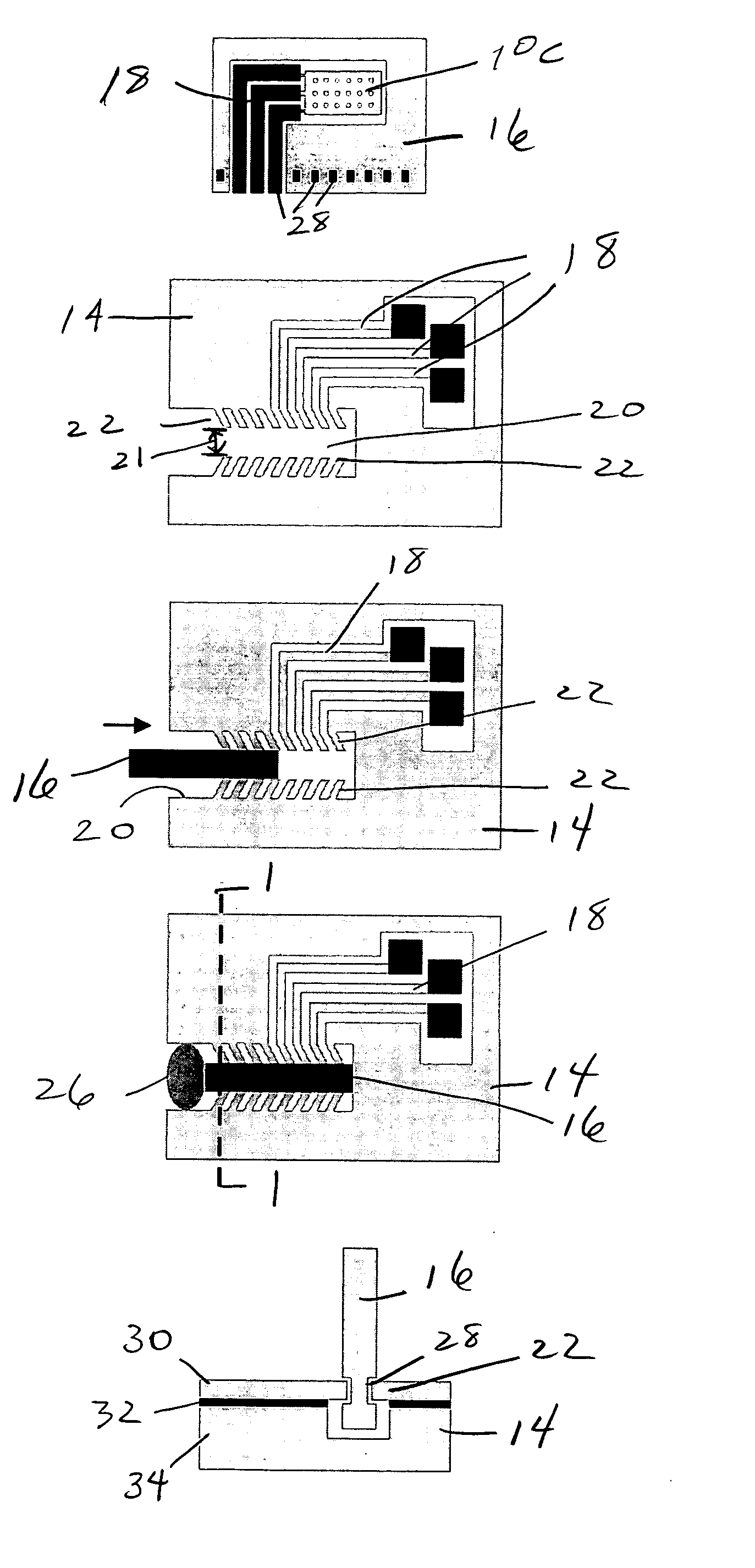
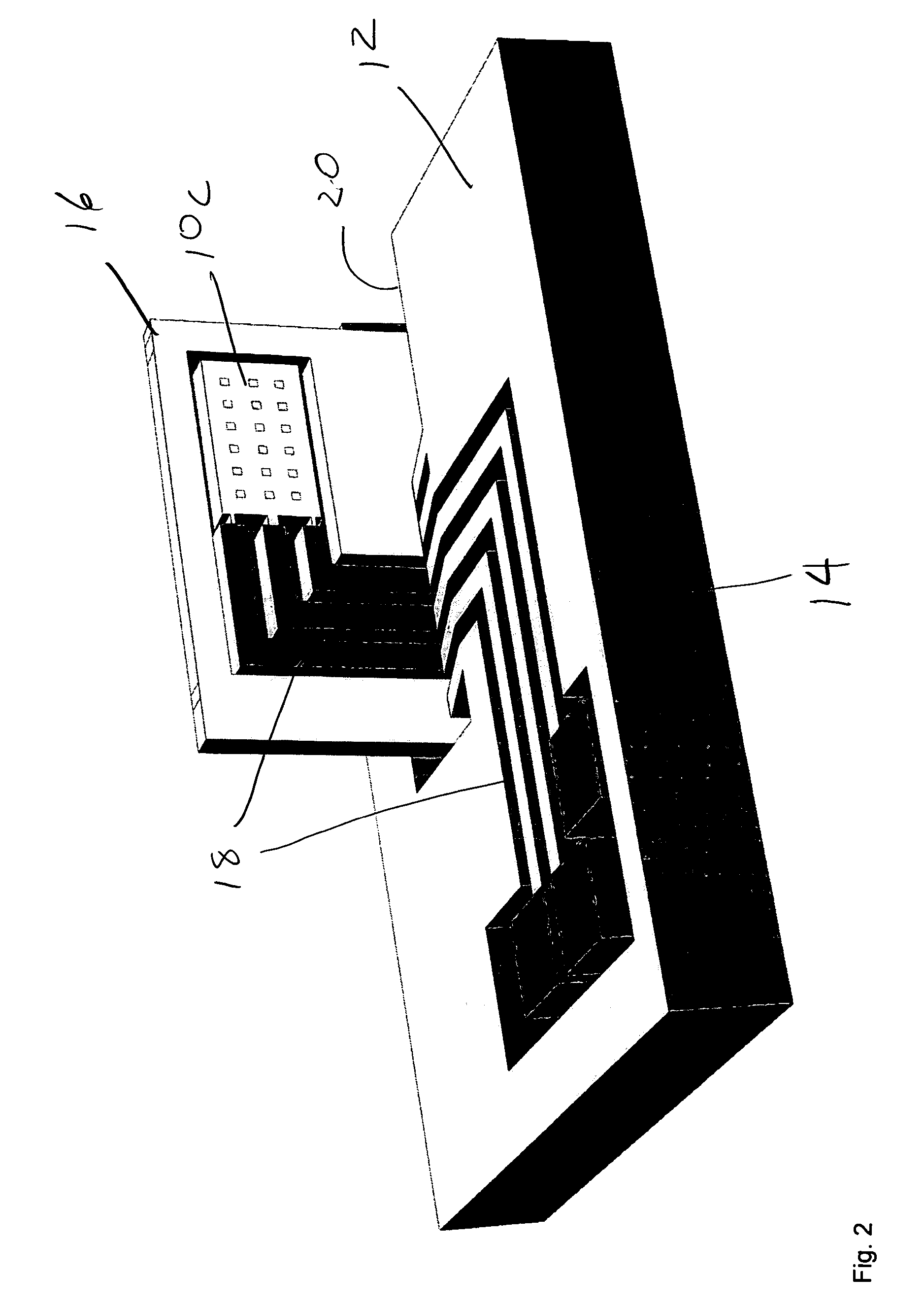
[0031] A method for assembling three-dimensional micromachined sensors or passive or active MEMS devices is disclosed. By etching a cavity 20 in silicon-on-insulator (SOI) wafers 14 and placing a second chip or wafer 16 vertically in the cavity 20, a three-dimensional structure can be constructed. In this specification the terms “wafer”, “chip” or “substrate” shall be interchangeably used as equivalents of each other. In addition to allowing for out-of-plane components on a wafer 16, this process enables post-fabrication assembly of three-axis sensors 24 as described below. Electrical conductors 18 can be provided on both the out-of-plane wafer 16 and the holder wafer 14 and coupled together with the assembly process.

[0032] To provide stable mounting, an SOI wafer 14 with a very thick device layer is preferably used (on the order of 100-500 μm). Alternatively, the cavity 20 can be defined in a handle layer of an SOI wafer 14. In some cases additional wafer bonding (e.g. Si-to-Si fu...


PUM


Abstract

A method of assembling a three dimensional micromachined structure comprising the steps of defining a cavity in a holder wafer having a thick upper layer, providing a plurality of fingers in the thick upper layer extending from the holder wafer into the cavity, and disposing an out-of-plane wafer into the cavity in the holder wafer in engagement with the fingers to hold the out-of-plane wafer in place in an out-of-plane position with respect to the holder wafer. The invention also includes an apparatus made according to any combination of the above method steps and/or the structure of the apparatus which is fabricated from any combination of those method steps.

Description

RELATED APPLICATIONS [0001] The present application is related to U.S. Provisional Patent Application, Ser. No. 60 / 726,684, filed on Oct. 13, 2005, and Ser. No. 60 / 726,723, filed on Oct. 13, 2005, which are incorporated herein by reference and to which priority is claimed pursuant to 35 USC 119.BACKGROUND OF THE INVENTION [0002] 1. Field of the Invention [0003] The invention relates to methods for the assembly of three dimensional microelectromechanical systems (MEMS). [0004] 2. Description of the Prior Art [0005] Microassembly techniques have been proposed for optical MEMS. In the publications listed below it is disclosed that a deposited layer of, for example, silicon carbide or silicon nitride serves as elastic flexures above a V-groove. Optical MEMS components can be inserted into the V-groove from the top and are held in place by the flexures. However, this method is only used for passive components. Further disclosure can be found in P. Boyle et.al., “Packaging solutions for M...

Claims


Application Information

Patent Timeline
Patent Type & Authority Applications(United States)
IPC IPC(8): H01L21/00H01L23/495
CPCB81B2201/025B81B2203/053B81B2203/055B81C3/008G01P1/023H01L2924/0002G01P15/0802G01P15/09H01L2924/00
Inventor EKLUND, E. JESPERSHKEL, ANDREI M.
Owner RGT UNIV OF CALIFORNIA
Why Eureka
Try Eureka