
Solar cell-driven display device and method of manufacturing thereof

a technology of solar cells and display devices, which is applied in the direction of sustainable manufacturing/processing, instruments, and final product manufacturing, etc., can solve the problems of high cost, complex manufacturing process, and inability to easily replace the cells of the display or connect electric power supply lines to the display, and achieves the effect of simplifying the process

Inactive Publication Date: 2007-04-26
SAMSUNG ELECTRONICS CO LTD
View PDF5 Cites 53 Cited by
  • Summary
  • Abstract
  • Description
  • Claims
  • Application Information

AI Technical Summary

Benefits of technology

[0011] The present invention further provides a solar cell-driven display device that functions both as a display device and as a light-emitting device and is manufactured using a simpler process.

Problems solved by technology

They are also sometimes installed in isolated areas where it is impossible to easily replace the cells of the displays or to connect electric power supply lines to the displays.
However, such display devices have a problem in that their volume greatly increases, because a solar cell panel and a display device panel, which have been separately manufactured, are generally assembled with each other.
Another problem is that their manufacturing process is complex and hence is expensive, due to the presence of circuits and interconnects between the solar cell and the display device.
However, the disclosed display device has problems in that the light guide plate is required as a separate element and circuits and interconnects for connecting the separate element to the light-emitting element and the display element are complex, thereby increasing manufacturing costs and complicating the manufacturing process.
However, this solar cell-integrated display device also has problems in that the existing display element has a complex structure that is physically connected, and separate elements such as the polymer film and a multi-layer insulating film are additionally formed, thus making the manufacturing process relatively complex.

Method used


Image

  • Solar cell-driven display device and method of manufacturing thereof
  • Solar cell-driven display device and method of manufacturing thereof
  • Solar cell-driven display device and method of manufacturing thereof

Examples


example

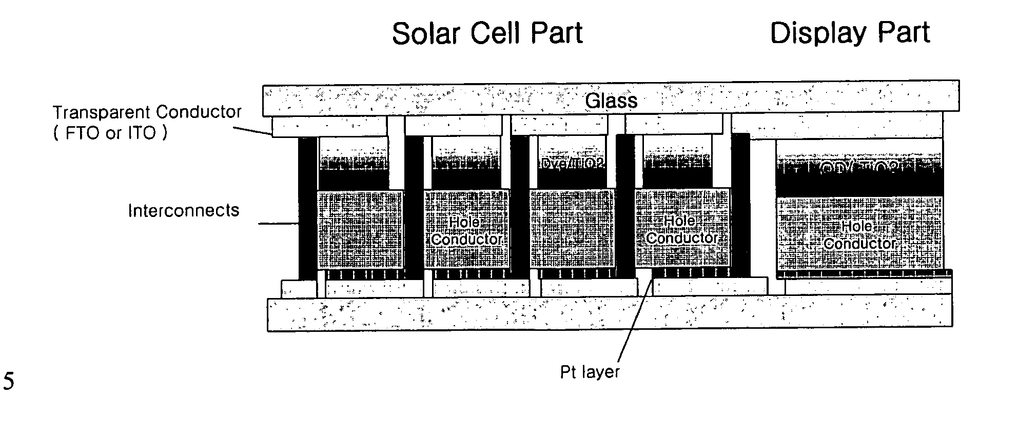
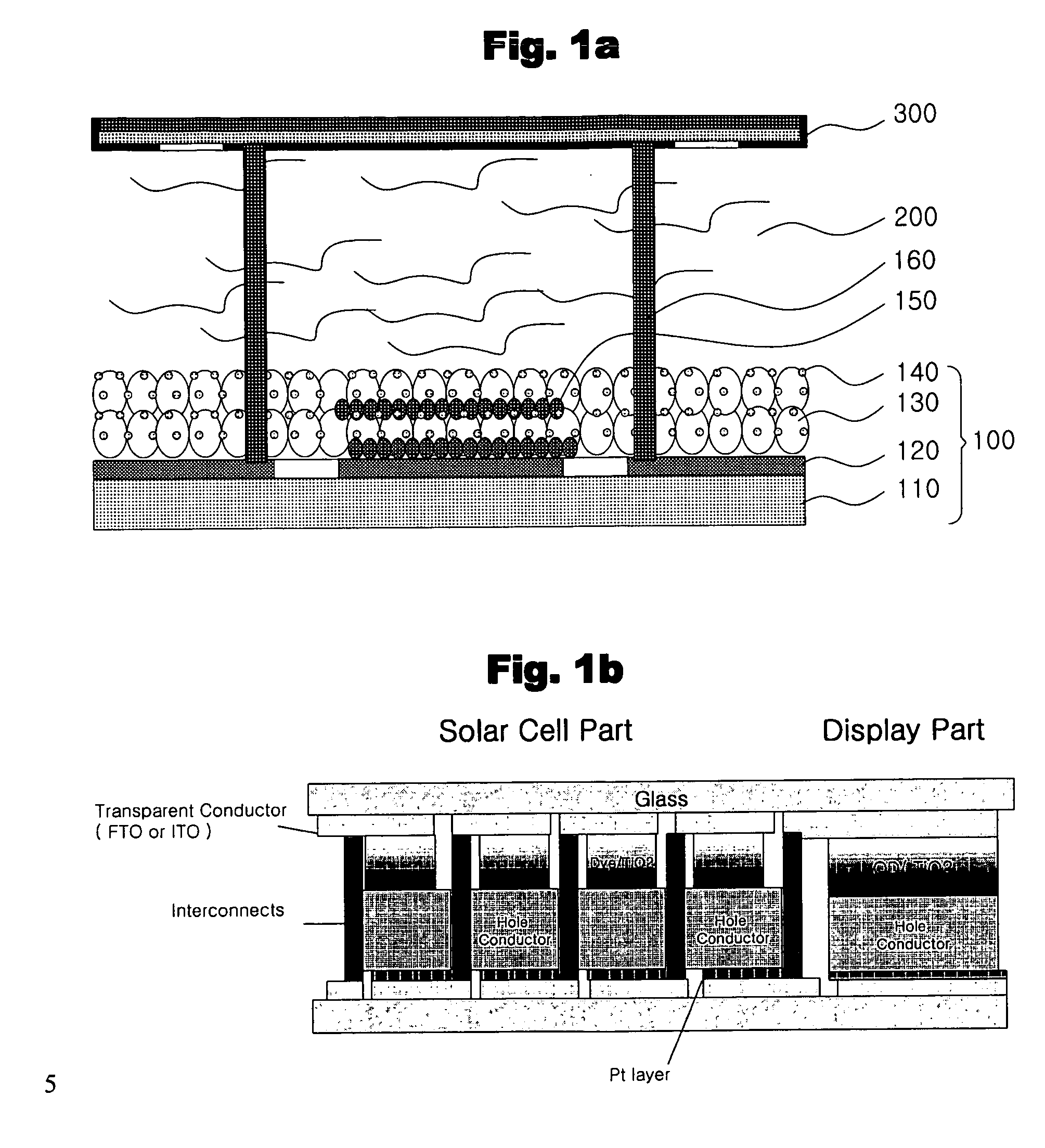
[0058] As shown in FIG. 1, fluorine-doped tin oxide (FTO) was deposited as a transparent electrode layer on a glass substrate. The electrode layer was etched to form patterns having a desired geometry. Then, on the FTO film, a paste of TiO2 (average size: 12 nm; commercially available under the trade name of Ti-nanoxide HTSP from Solaronix SA) was screen-printed, and calcined at 500° C. for 30 minutes to form a 12 micrometer (μm) thick semiconductor layer. Next, the resulting substrate was dipped in 0.3 millimolar (mM) ruthenium dithiocyanate 2,2′-bipyridyl-4,4′-dicarboxylate solution for 12 hours and dried so as to adsorb the dye on the surface of the TiO2 layer.

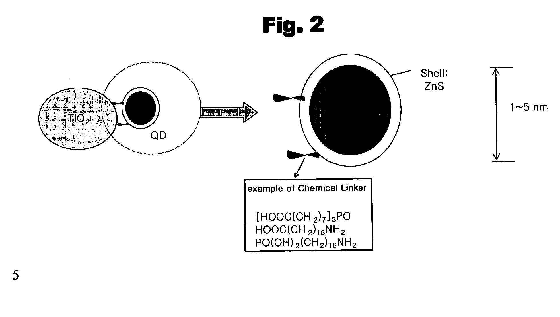
[0059] A quantum dot compound having a particle size distribution of about 3 to about 5 nm and a core-shell structure of CdSe—ZnS was surface-treated with tri-(1-carboxy)heptylphosphine oxide and then dispersed in an alcohol solution. The quantum dot light-emitting layer solution was printed on a display portion and dried ...


PUM

PropertyMeasurementUnit
Sizeaaaaaaaaaa
Transparencyaaaaaaaaaa
Transport propertiesaaaaaaaaaa

Abstract

Disclosed herein are a solar cell-driven display device wherein a dye-sensitized solar cell, which comprises a light-absorbing layer that comprises a semiconductor electrode including a transparent electrode formed on a substrate and nanocrystals adsorbed with a photosensitive dye on the transparent electrode, and a hole transport layer and a counter electrode, is formed so as to exhibit a display device function using a quantum dot light-emitting layer, as well as a manufacturing method thereof. The solar cell-driven display device exhibits the display device function using only solar light, without needing a separate power supply device, and thus can be applied to advertising displays in isolated areas or as other outdoor advertising displays.

Description

BACKGROUND OF THE INVENTION [0001] This non-provisional application claims priority under 35 U.S.C. § 119(a) to Korean Patent Application No. 2005-101357 filed on Oct. 26, 2005, the entire contents of which are hereby incorporated by reference. [0002] 1. Field of the Invention [0003] The present invention relates to a solar cell-driven display device and a method of manufacturing thereof. More particularly, the present invention relates to a solar cell-driven display device comprising a transparent electrode formed on a substrate, a light-absorbing layer formed on the transparent electrode, a hole transport layer, and a counter electrode. A quantum dot light-emitting layer is formed on the surface of the light-absorbing layer. [0004] 2. Description of the Prior Art [0005] Various display devices have recently been developed for outdoor advertising displays and the like. Such advertising displays are often placed on the roofs of buildings and the like. They are also sometimes install...

Claims


Application Information

Patent Timeline
IPC IPC(8): H01L31/00G09G3/06
CPCB82Y10/00B82Y20/00B82Y30/00H01G9/2009H01G9/2031H01G9/2059H01L27/3227H01L27/3239H01L51/0035H01L51/0036H01L51/0086H01L51/502Y02E10/542Y02P70/50H10K59/221H10K59/60H10K85/113H10K85/111H10K85/344H10K50/115H05B33/12C09K11/06H05B33/10
Inventor NOH, CHANG HOCHO, SUNG HENSONG, KI YONGKIM, JIN YOUNGKIM, JONG MIN
Owner SAMSUNG ELECTRONICS CO LTD
Learn More