Semiconductor device and a method of testing the same

a technology of semiconductor devices and semiconductors, applied in the direction of individual semiconductor device testing, semiconductor/solid-state device testing/measurement, instruments, etc., can solve the problems of increasing test costs and reducing product costs, and achieves speed-up the test, reduce the cost of testing, and increase the circuit area

Inactive Publication Date: 2007-04-26
RENESAS ELECTRONICS CORP
View PDF8 Cites 5 Cited by
  • Summary
  • Abstract
  • Description
  • Claims
  • Application Information

AI Technical Summary

Benefits of technology

[0020] In accordance with the present invention, it is possible to speed-up the test.
[0021] In accordance with the present in

Problems solved by technology

As a result, an increase in the test cost is introduced

Method used


Image

  • Semiconductor device and a method of testing the same
  • Semiconductor device and a method of testing the same
  • Semiconductor device and a method of testing the same

Examples


Embodiment Construction

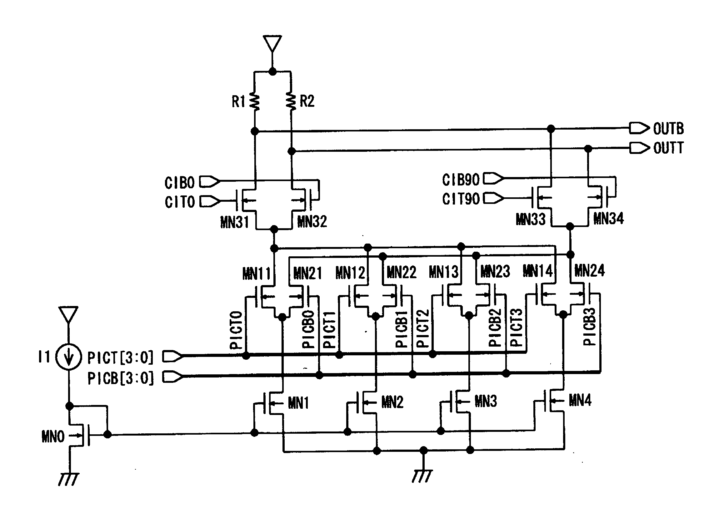
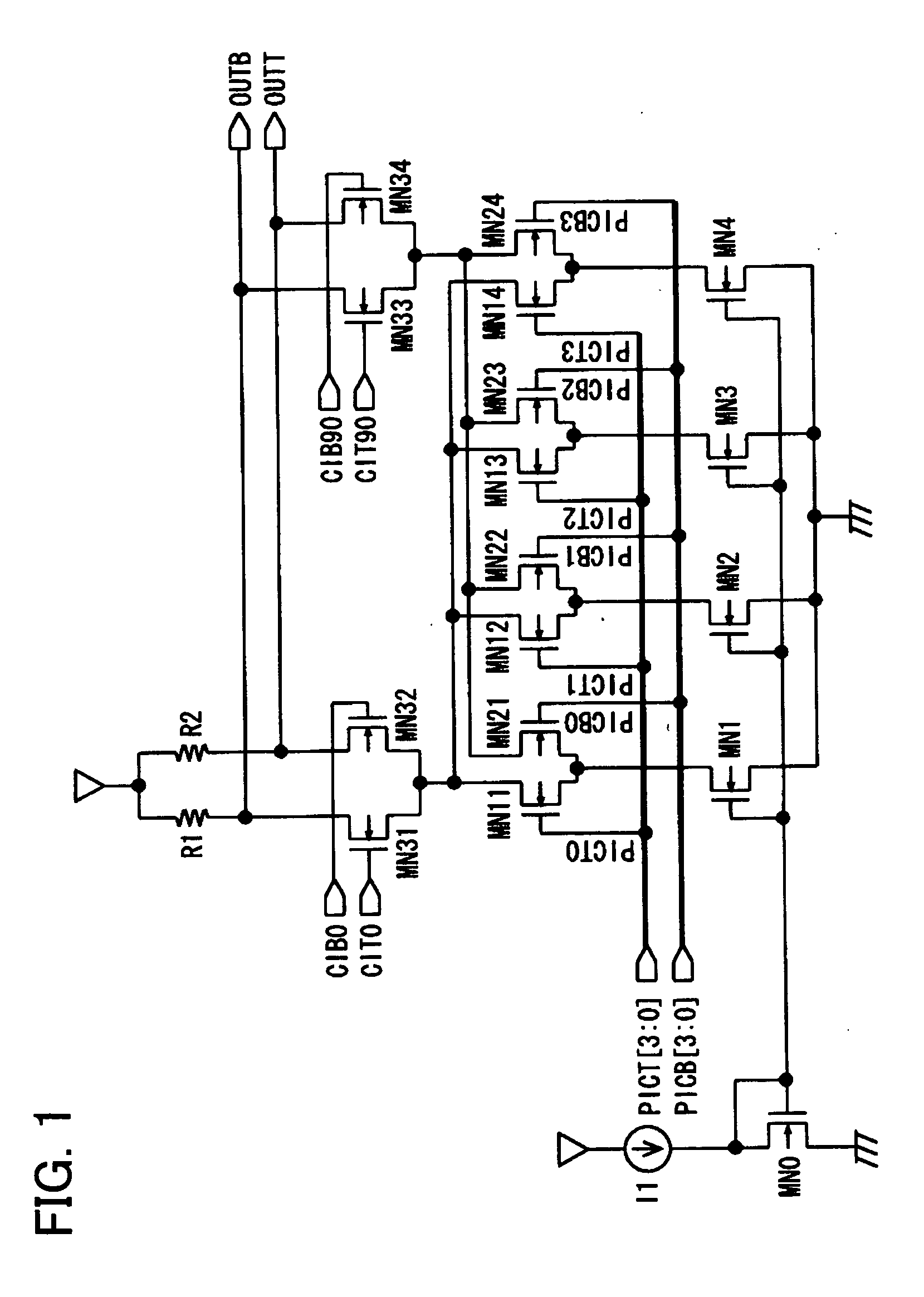
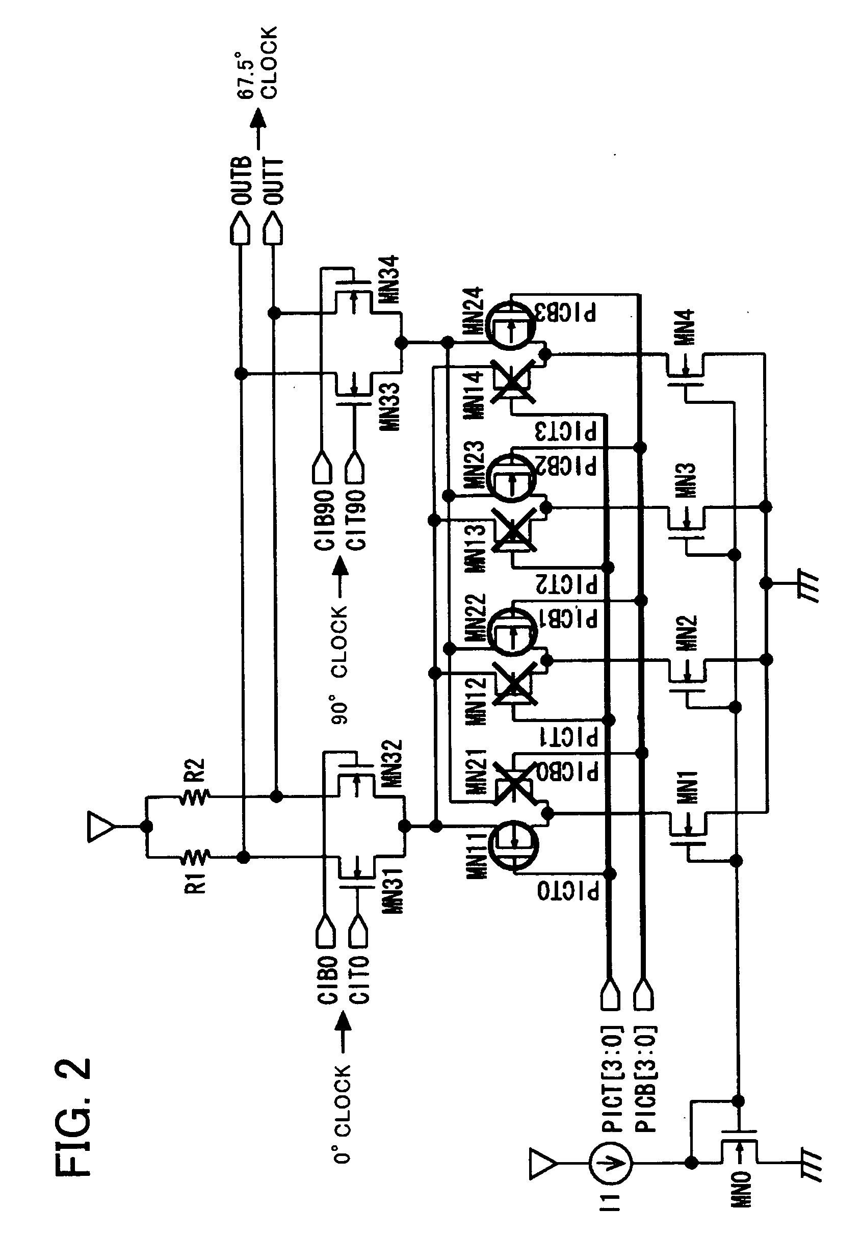
[0028] The above-mentioned present invention will now be described in detail with reference to annexed drawings: FIG. 1 is a view showing the configuration of one embodiment of the present invention. In FIG. 1, elements which are identical with those in FIG. 6 are denoted by identical references. Referring now to FIG. 1, in one embodiment of the present invention, control signals PCT0, PCT1, PCT2, PCT3 are connected to the gates of NMOS transistors MN11, MN12, MN13, MN14 of first to fourth switch pairs, respectively, and control signals PIC0, PIC1, PIC2, PIC3 are connected to the gates of other NMOS transistors MN21, MN22, MN23, MN24 of the first to fourth switch pairs, respectively. The NMOS transistors MN11, MN12, MN13, MN14; MN21, MN22, MN23, MN24 can be controlled with a four-bit control signal PICT [3:0] and four-bit control signal PICB [3:0], so that they are turned on or off, individually. Such a circuit configuration of the present invention obviates the necessity of dedicat...


PUM


Abstract

The present invention comprises first and second differential pairs (MN31, MN32), (MN33, MN34) to which first and second differential input signals (CIB0, CIT0), (CIB90, CIT90) are input, output pairs of said first and second differential pairs being commonly connected to each other, further connected to load circuits (MN1 to MN4) and connected to differential output terminals (OUTT, OUTB); first to fourth current sources (MN1 to MN4); and first to fourth switch pairs (MN11, MN21), (MN12, MN22), (MN13, MN23), (MN14, MN24). Switches on one side of said first to N-th switch pairs are connected at one end thereof to said first to fourth current sources and are commonly connected at the other end thereof to said second differential pair. Control signals PICT [3:0], PICB [4:0] are connected to control terminals of said first to N-th switch pairs, so that a pattern is applied to the control signal. The operation of the current sources can be confirmed by a functional test in which output signals are compared with expected values.

Description

FIELD OF THE INVENTION [0001] The present invention relates to a semiconductor device and in particular to an apparatus having a configuration which is preferable for testing said semiconductor device and a method for testing the same. BACKGROUND OF THE INVENTION [0002] An exemplary structure of typical phase interpolator is shown in FIG. 6. The phase interpolator is adapted to output in response to a control signal, output signals each having a phase corresponding to any of phases which are obtained by dividing the difference in phase between two input signals. A configuration is shown in FIG. 6 in which the phase difference between two input signals is divided into four regions, so that output signals corresponding to any of phases are output in response to a control signal. [0003] Referring now to FIG. 6, the phase interpolator comprises a first differential pair of transistors (NMOS transistor pair MN31, MN32) to which first differential input signals (phase 0°) (CIB 0, CIT 0) a...

Claims


Application Information

Patent Timeline
IPC IPC(8): G11C7/02G01R31/28H01L21/822H01L27/04
CPCG01R31/31725G01R31/26H01L22/00H01L27/04
Inventor SAKAI, SHINGO
Owner RENESAS ELECTRONICS CORP
Why Eureka
Try Eureka