Screen printing using nanoporous polymeric membranes and conductive inks

a nanoporous polymer membrane and conductive ink technology, applied in the field of screen printing, can solve the problems of non-standard edges, undesirable varying widths, and low screen printing efficiency, and achieve the effects of reducing the pore size of the screen, widening the application of printing, and high resolution

Inactive Publication Date: 2007-04-26
SOLIGIE
View PDF12 Cites 3 Cited by
  • Summary
  • Abstract
  • Description
  • Claims
  • Application Information

AI Technical Summary

Benefits of technology

[0009] According to embodiments of the present invention, a dramatic reduction in pore size of screens and conductive particles in inks improves and broadens applications for printing with conductive and other inks with high resolution. Such applications include the additive printing of electrical components such as, for example, conductive, semiconductive, and dielectric traces. In various embodiments, the electrical components can include circuits, transistors, antennae, and the like.

Problems solved by technology

Screen printing, however, is typically not an option for the printing of electrical components because of current screen technology, wherein screens have relatively large pore sizes, i.e., greater than one micron in diameter.
Further, conductive inks typically comprise relatively large conductive particles of silver, copper, and other materials, again on the order of one micron in diameter or greater, which may be compatible with screen pore sizes but do not provide the desired fine-scale printed results.
The use of current screens in high resolution applications therefore produces electrical traces and components with non-uniform edges and undesirable varying widths because the individual pore sizes of the screen constitute a significant portion of the desired electrical trace being printed.

Method used


Image

  • Screen printing using nanoporous polymeric membranes and conductive inks
  • Screen printing using nanoporous polymeric membranes and conductive inks
  • Screen printing using nanoporous polymeric membranes and conductive inks

Examples


Embodiment Construction

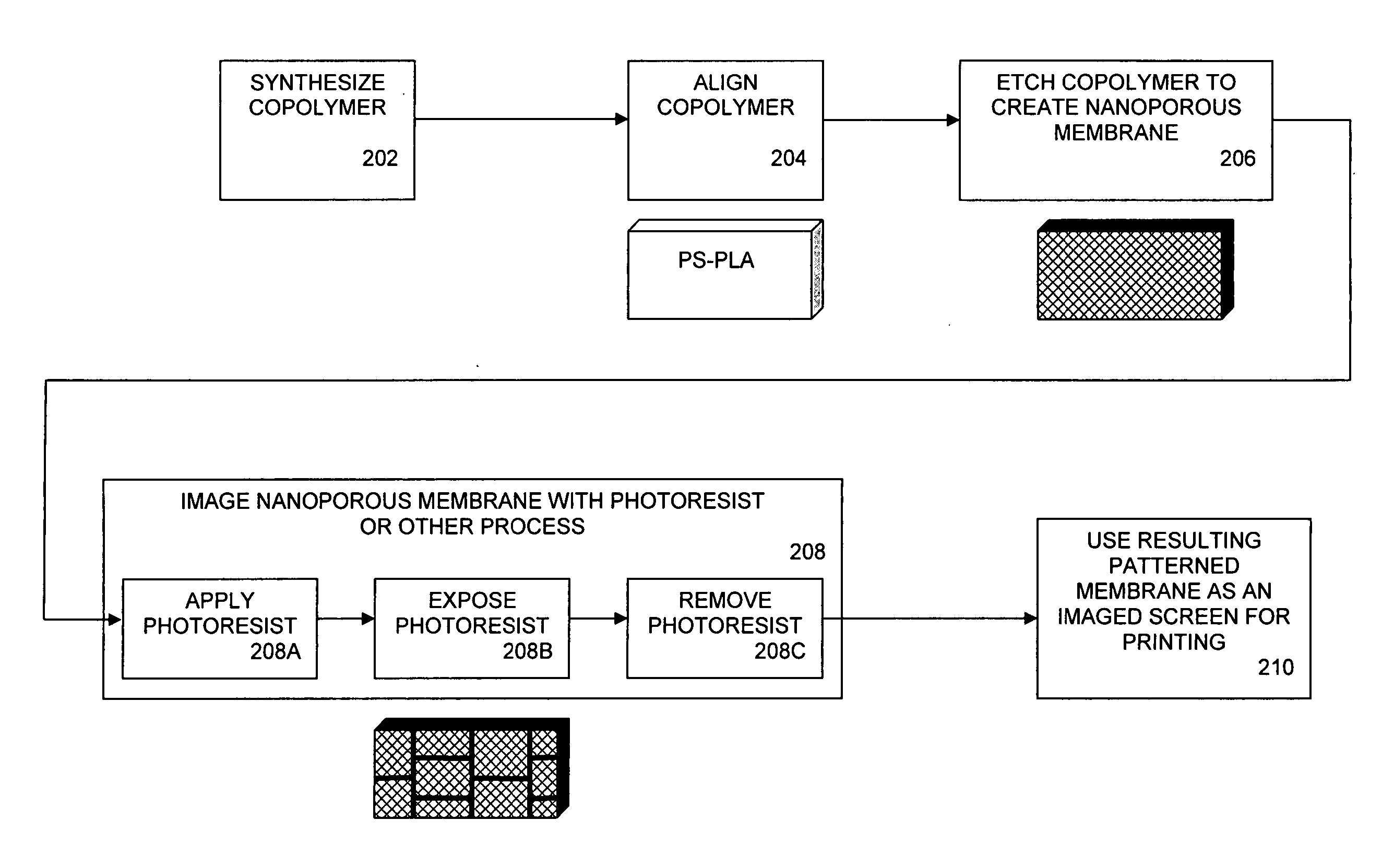
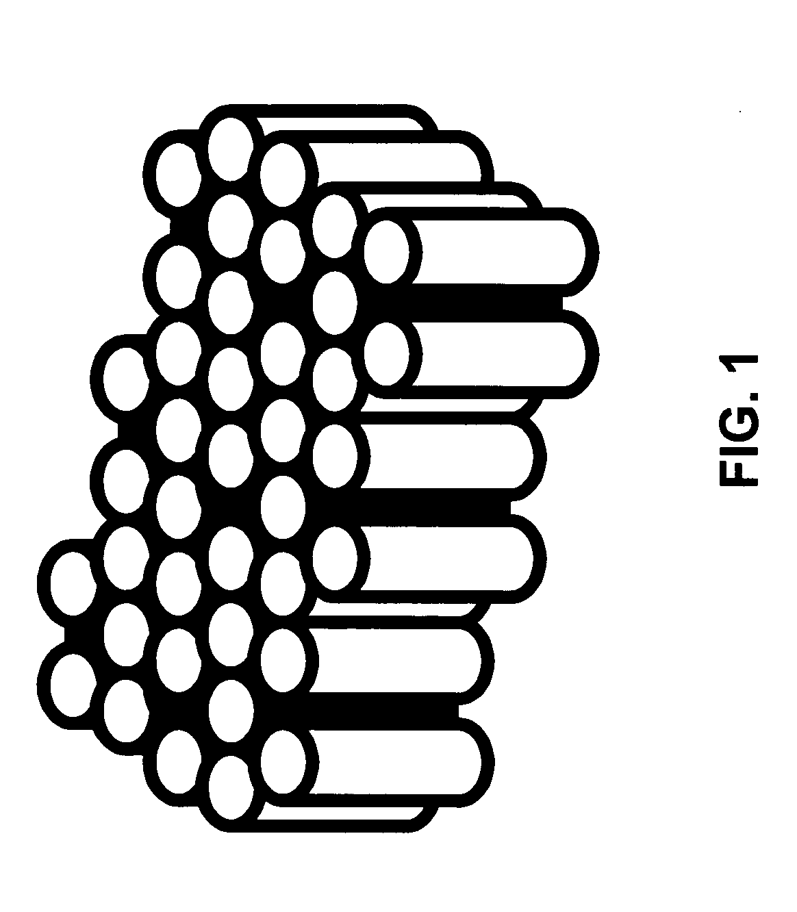
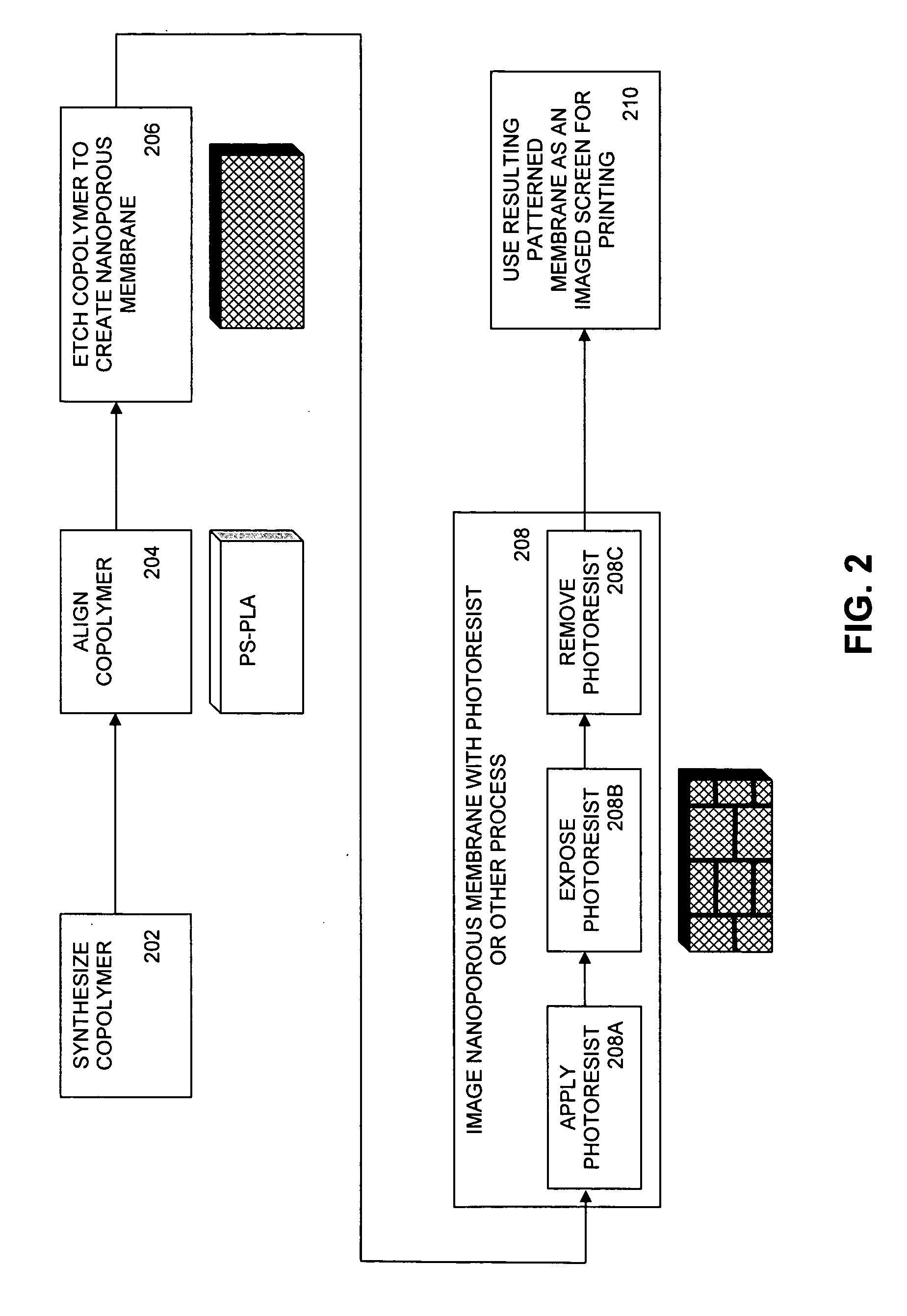
[0016] Electrical components manufactured by additive printing processes require high resolution printing techniques. High resolution printed images and articles are often difficult to achieve with commercial printing techniques, such as screen printing. The novel combination of nanoporous polymeric membrane technology with conductive inks having small particle size results in the ability to screen print electrical components with adequate resolution. The invention thereby enables screen printing with resolutions of less than about 200 microns, preferably about 25 microns or less, in various embodiments.

[0017] In one embodiment, the method of the invention includes creating a porous membrane through a chemical process. The membrane is then patterned and pores are etched according to a desired pattern. The membrane may then be used to pattern conductive traces on a substrate according to a screen printing or other suitable printing technique.

[0018] New materials are emerging, drive...


PUM

PropertyMeasurementUnit
diameteraaaaaaaaaa
diameteraaaaaaaaaa
widthaaaaaaaaaa

Abstract

Screen printing methods, processes, apparatuses, and techniques using nanoporous polymeric membranes, and electrical components, such as traces, transistors, circuits, assemblies, and the like additively printed utilizing nanoporous membranes. In one embodiment, the invention includes creating a nanoporous membrane through a chemical process. The membrane is patterned and pores are etched according to a desired pattern. The membrane may then be used to pattern conductive traces on a substrate according to a screen printing or other suitable printing technique.

Description

RELATED APPLICATION [0001] This application claims the benefit of U.S. Provisional Application No. 60 / 720,018, filed Sep. 23, 2005, which is incorporated herein by reference in its entirety.FIELD OF INVENTION [0002] The invention relates generally to screen printing. More particularly, the invention relates to screen printing using nanoporous polymeric membranes and conductive inks to additively create electrical and other components. BACKGROUND OF INVENTION [0003] Screen printing is commonly known in the printing industry as a means for transferring inks onto a substrate. Screen printing is used in many different applications in printing such as, for example, printing of T-shirts, greeting cards, and other printing applications involving an ink transfer. Screens used in screen printing today are typically constructed of a fine nylon mesh having openings that can range from as large as about 200 microns or more to as fine as about 25 microns in diameter, stretched over an aluminum o...

Claims


Application Information

Patent Timeline
Patent Type & Authority Applications(United States)
IPC IPC(8): B05C1/00B05D3/12
CPCB01D67/0034B01D67/0062B01D71/021B01D71/027B01D71/28B05D1/32B41C1/14B41C1/148B41M1/12B41M3/006B41N1/247B82Y10/00G03F7/12H05K3/1225H05K2201/0116H05K2201/0257B01D71/76B01D2323/345B01D2325/08B01D2325/38B01D71/281
Inventor TIMM, MATTHEW P.DEROCHER, JONATHAN
Owner SOLIGIE
Why Eureka
Try Eureka