Nitride semiconductor light emitting device and method for manufacturing the same

a light-emitting device and semiconductor technology, applied in the direction of semiconductor devices, basic electric elements, electrical equipment, etc., can solve the problems of affecting the operation voltage, and reducing the overall light-emitting efficiency, so as to improve the operating voltage characteristics, improve the light-emitting efficiency, and the effect of resistance to esd

Inactive Publication Date: 2007-05-03
SAMSUNG ELECTRO MECHANICS CO LTD
View PDF4 Cites 23 Cited by
  • Summary
  • Abstract
  • Description
  • Claims
  • Application Information

AI Technical Summary

Benefits of technology

[0009] The present invention has been made to solve the foregoing problems of the prior art and therefore an object of certain embodiments of the present invention is to provide a nitride semiconductor light emitting device having improved light emission efficiency, operating voltage characteristics and resistance to ESD due to a current spreading effect.
[0010] Another object of certain embodiments of the invention is to provide a method of manufacturing a nitride semiconductor light emitting device that can improve light emission efficiency, operating voltage characteristics and resistance to ESD thereof.
[0018] According to an embodiment of the present invention, the nitride semiconductor light emitting device may further comprise a contact metal layer between the p-type nitride semiconductor layer and the transparent conductive oxide multi-layer. The contact metal layer may be made of at least one selected from a group consisting of Ni, Au, Pt and Pd. The contact metal layer functions to further enhance ohmic contact characteristics with the p-type nitride semiconductor layer.

Problems solved by technology

However, the Ni / Au layer has a low light transmittance, thus degrading overall light emission efficiency.
However, the transparent electrode 18 made of Ni / Au has a low light transmittance of about 60% in the wavelength range of light generated from the active layer 14, thus resulting in low light emission efficiency.
Still however, the ITO transparent electrode does not form a good ohmic contact with the p-type nitride semiconductor, thus adversely increasing the operating voltage.
However, according to the above-described conventional technologies, current tends to concentrate in the region where a p-side bonding electrode is formed, causing non-uniform light emission characteristics.
Also, due to the locally concentrated current, the light emitting device is vulnerable to ESD.

Method used


Image

  • Nitride semiconductor light emitting device and method for manufacturing the same
  • Nitride semiconductor light emitting device and method for manufacturing the same
  • Nitride semiconductor light emitting device and method for manufacturing the same

Examples


Embodiment Construction

[0037] Preferred embodiments of the present invention will now be described in detail with reference to the accompanying drawings. The invention may however be embodied in many different forms and should not be construed as limited to the embodiments set forth herein. Rather, these embodiments are provided so that this disclosure will be thorough and complete, and will fully convey the scope of the invention to those skilled in the art. In the drawings, the shapes and dimensions are exaggerated for clarity and the same reference numerals are used throughout to designate the same components.

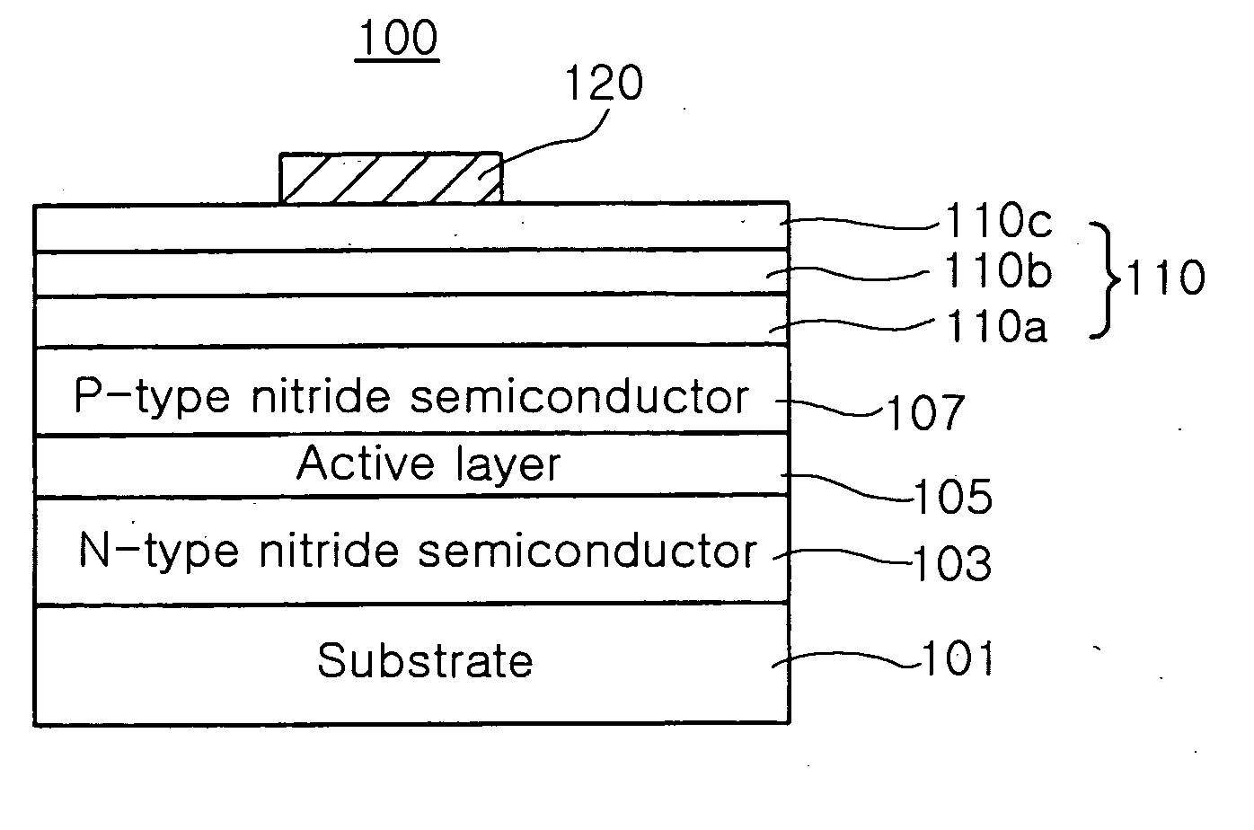
[0038]FIG. 3 is a sectional view illustrating a nitride semiconductor light emitting device according to an embodiment of the present invention. Referring to FIG. 3, the nitride semiconductor light emitting device 100 includes an n-type nitride semiconductor layer 103, an active layer 105 and a p-type nitride semiconductor layer 107 sequentially formed on a substrate 101 made of sapphire, etc. On...


PUM


Abstract

The invention relates to a nitride semiconductor light emitting device having a high light emission efficiency, low operating voltage and high resistance to electrostatic discharge. The nitride semiconductor light emitting device includes an n-type nitride semiconductor layer, an active layer and a p-type nitride semiconductor layer formed in their order on a substrate. The device also includes a transparent conductive oxide multi-layer formed on the p-type nitride semiconductor layer. The transparent conductive oxide multi-layer includes two or more layers or transparent conductive oxide layers having different levels of conductivity.

Description

CLAIM OF PRIORITY [0001] This application claims the benefit of Korean Patent Application No. 2005-83726 filed on Sep. 8, 2005, in the Korean Intellectual Property Office, the disclosure of which is incorporated herein by reference. BACKGROUND OF THE INVENTION [0002] 1. Field of the Invention [0003] The present invention relates to a nitride semiconductor light emitting device, and more particularly, to a nitride semiconductor light emitting device having high light emission efficiency while having low operating voltage and high resistance to Electrostatic Discharge (ESD). [0004] 2. Description of the Related Art [0005] Recently, light emitting diodes (LEDs) or laser diodes (LDs) using group III-V nitride semiconductors (or simply nitride semiconductors) are extensively adopted in light emitting devices to obtain light in blue or green wavelength range and applied to various products such as display boards, illumination apparatuses, etc. as light sources therefor. The group III-V ni...

Claims


Application Information

Patent Timeline
Patent Type & Authority Applications(United States)
IPC IPC(8): H01L33/00H01L29/24H01L33/32H01L33/42
CPCH01L33/32H01L33/40H01L33/42
Inventor KIM, SUN WOONKIM, JE WONKANG, PIL GEUNSONG, KEUN MAN
Owner SAMSUNG ELECTRO MECHANICS CO LTD
Why Eureka
Try Eureka