Semiconductor device and a method of manufacturing the same

Inactive Publication Date: 2007-05-03
RENESAS TECH CORP
View PDF9 Cites 34 Cited by
  • Summary
  • Abstract
  • Description
  • Claims
  • Application Information

AI Technical Summary

Benefits of technology

[0021] A sealing body formed by resin molding is formed on a wiring substrate at the lowest stage, thereby a curing shrinkage effect of sealing resin occurs during the resin molding, and thus warp of the wiring substrate can be reduced. As a result, packaging performance can be improved in stacking of packages. Moreover, a film member is disposed on a surface of the sealing body o

Problems solved by technology

In this case, when one of the semiconductor chips is determined as a bad chip, for example, in a burn-in test after assembling the package, the semiconductor package as a whole is regarded as a bad package.
Furthermore, when a chip having the same size or a larger size is stacked at an upper stage, a method of stacking chips is restricted, for example, a spacer is required between chips, consequently stacking is often difficult.
That is, it was found that in the package structure described in the patent literature 1, since a glass epoxy substrate was used for a wiring substrate at a first stage (the lowest stage), there was a difficulty of occurre

Method used


Image

  • Semiconductor device and a method of manufacturing the same
  • Semiconductor device and a method of manufacturing the same
  • Semiconductor device and a method of manufacturing the same

Examples


embodiment

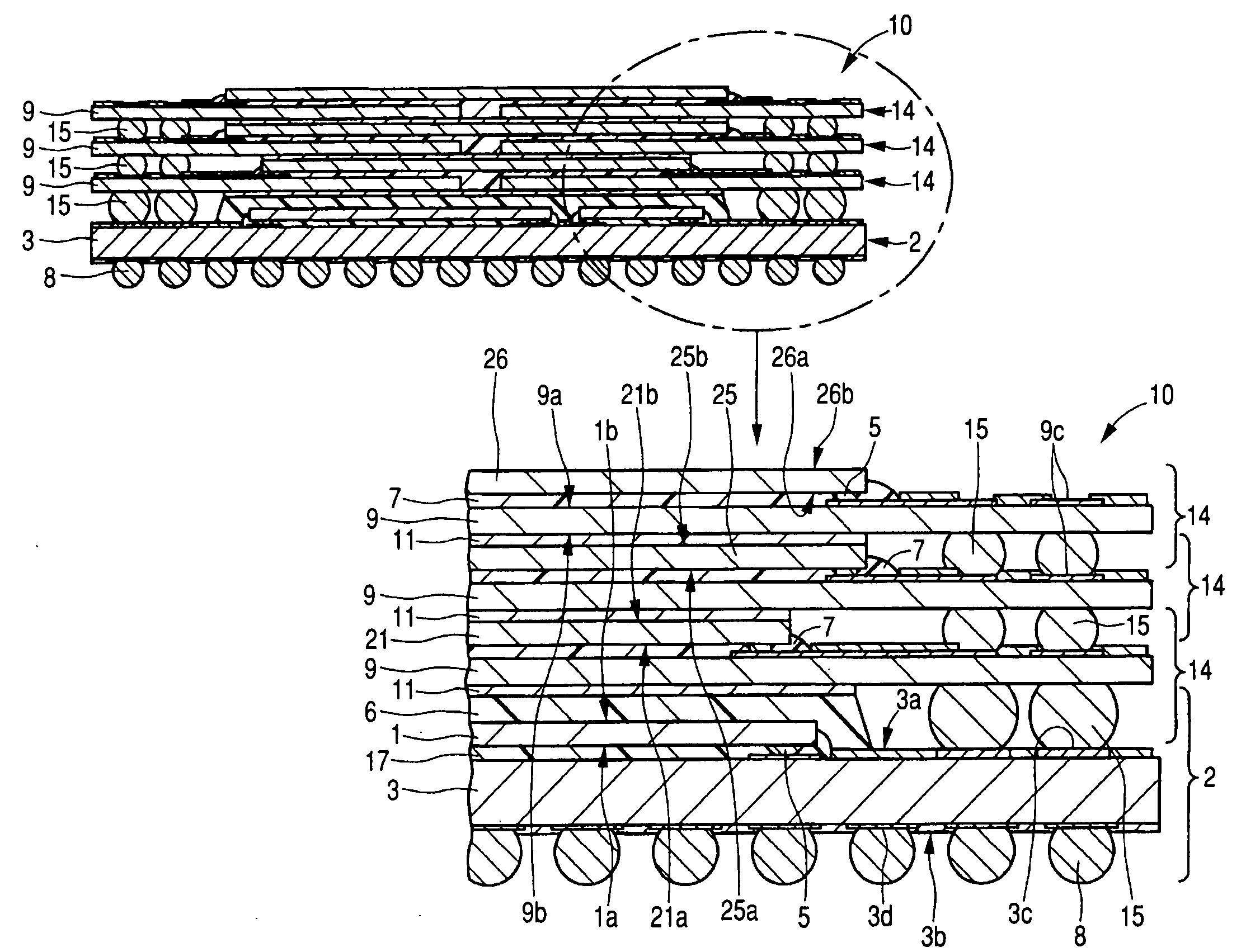
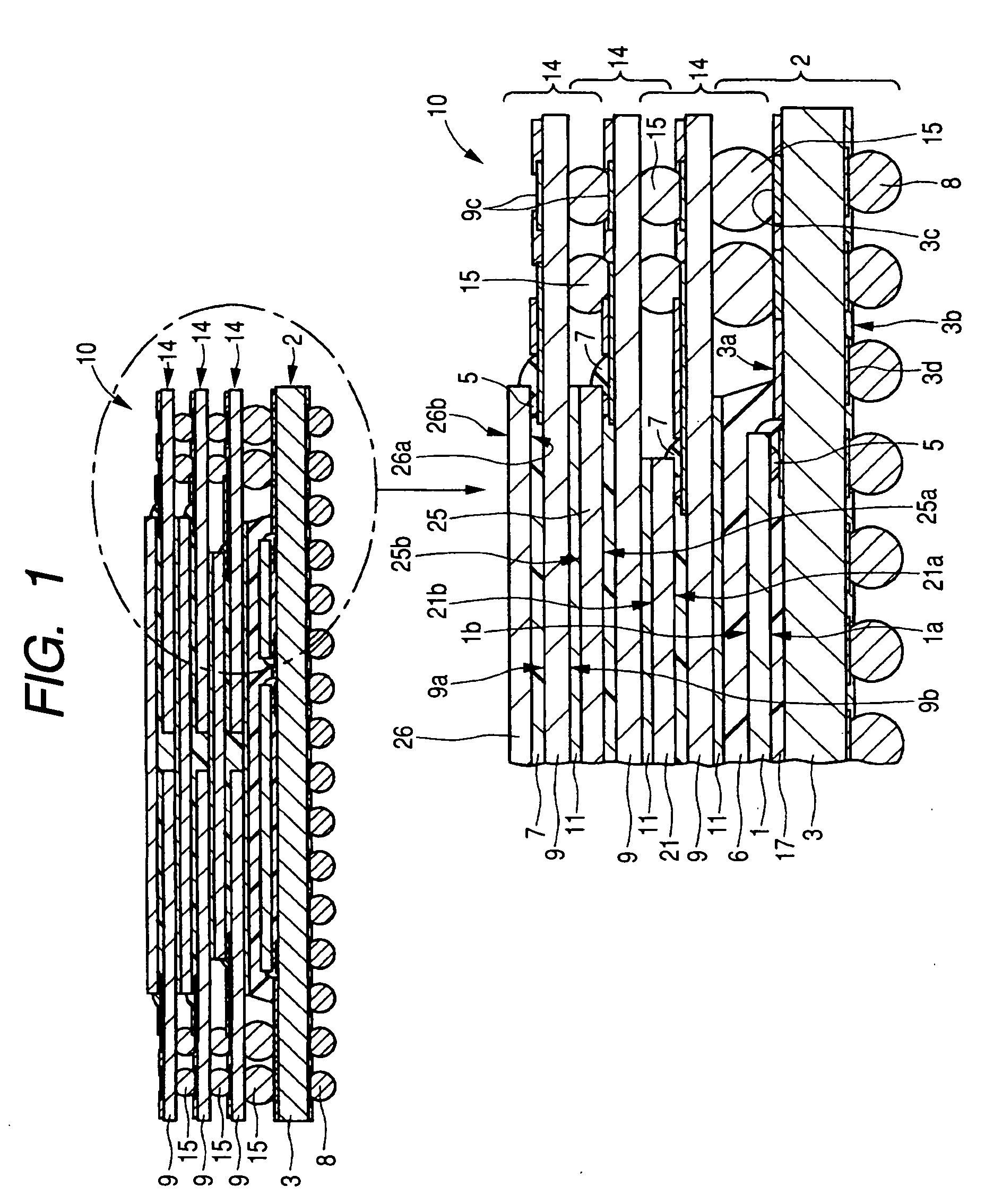
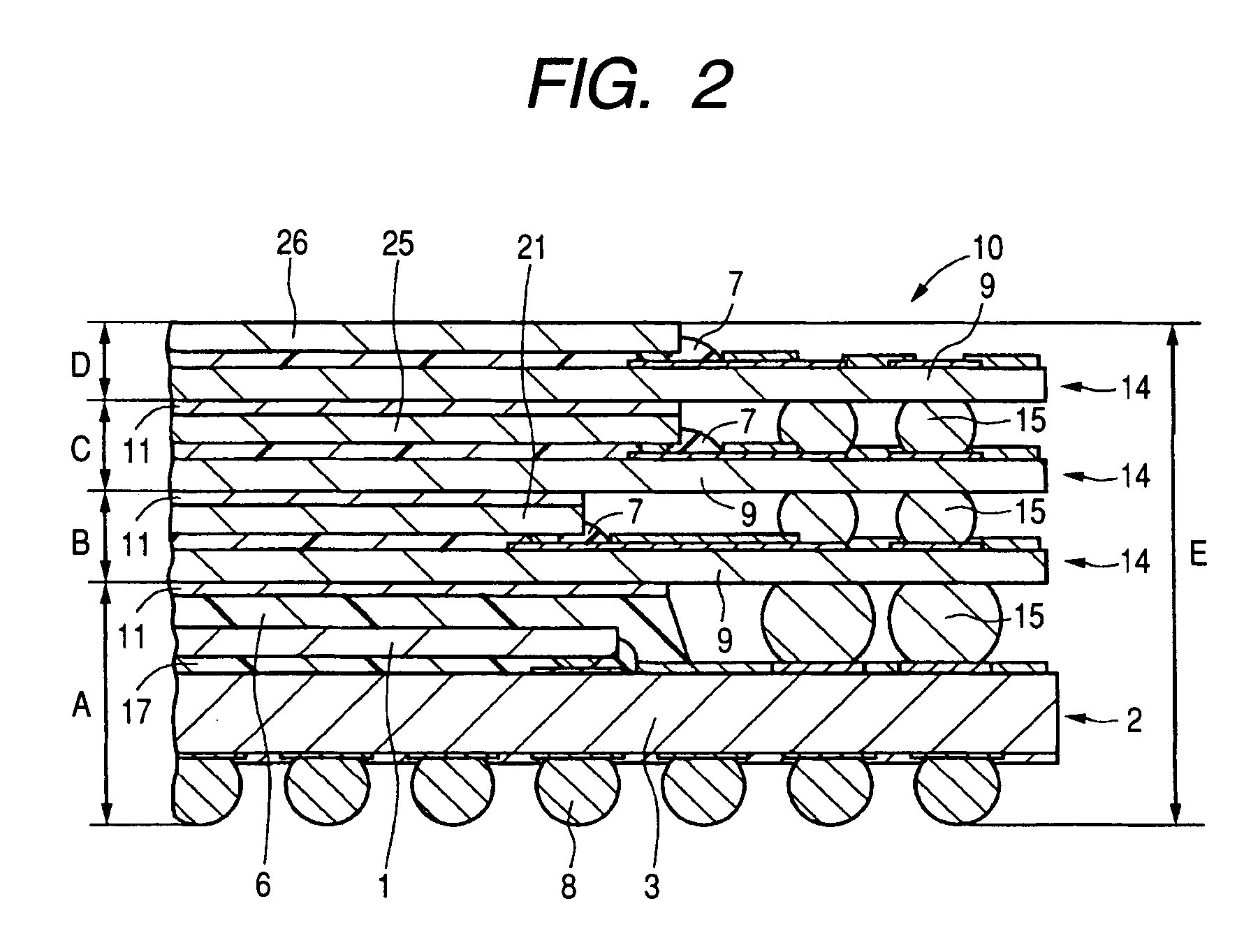
[0051]FIG. 1 shows a cross section view and an enlarged partial section view, showing an example of a structure of a semiconductor device of the embodiment of the invention, FIG. 2 shows an enlarged partial section view showing an example of thickness of each package of the semiconductor device shown in FIG. 1, FIG. 3 shows a data diagram showing an example of a numeral value of thickness of each member of the structure shown in FIG. 2, and FIG. 4 shows a plane view showing an example of a chip layout of a first semiconductor package at a first stage of the semiconductor device shown in FIG. 1. Furthermore, FIG. 5 shows a plane view showing an example of a chip layout of a second semiconductor package at a second stage of the semiconductor device shown in FIG. 1, FIG. 6 shows a plane view showing an example of a chip layout of second semiconductor packages at third and fourth stages of the semiconductor device shown in FIG. 1, and FIG. 7 shows a cross section view showing an example...


PUM


Abstract

Packaging performance of a semiconductor device is improved. A semiconductor device has a package substrate having a base material formed of resin; a semiconductor chip mounted on a main surface of the package substrate; a tape substrates being stacked on the package substrate in several stages, and electrically connected to a substrate at a lower stage via a plurality of solder balls; a second-stage chip, third-stage chip, and fourth-stage chip mounted on the tape substrates at respective stages; and a plurality of solder balls provided on a back surface of the package substrate; wherein a sealing body, which resin-seals the semiconductor chip and is formed by resin molding, is formed on a main surface of a package substrate disposed at the lowest stage, and the sealing body is disposed between the package substrate at the lowest stage and the tape substrate stacked thereon.

Description

CROSS-REFERENCE TO RELATED APPLICATIONS [0001] The disclosure of Japanese Patent Application No. 2005-312116 filed on Oct. 27, 2005 including the specification, drawings and abstract is incorporated herein by reference in its entirety. BACKGROUND OF THE INVENTION [0002] 1. Field of the Invention [0003] The present invention relates to a semiconductor device, and particularly relates to an effective technique for use in a semiconductor device having a structure of stacking semiconductor packages in multiple stages. [0004] 2. Description of Related Art [0005] A technique is given, which includes a multilayer substrate, a first-stage chip electrically connected to the multilayer substrate, different package substrates stacked on the multilayer substrate in three stages, each of which is connected to a wiring substrate at a lower stage via solder balls respectively, a second-stage chip, third-stage chip, and fourth-stage chip mounted on the different package substrates stacked in three ...

Claims


Application Information

Patent Timeline
IPC IPC(8): H01L23/02
CPCH01L24/81H01L2225/1023H01L25/50H01L2224/13144H01L2224/16H01L2224/8121H01L2224/81815H01L2224/83192H01L2924/01078H01L2924/01079H01L2924/15311H01L2924/3511H01L2924/01019H01L2224/16225H01L2224/32225H01L2224/73204H01L25/105H01L2224/73253H01L2924/15331H01L2225/1058H01L2924/00H01L25/10
Inventor ARAKI, MAKOTOGOTO, MASAKATSUNAKAMURA, SHIGERU
Owner RENESAS TECH CORP
Why Eureka
Try Eureka