


Quick Research
Generate reliable direction feasibility study reports for your R&D in just a few steps.

Technical Q&A
Discover and master advanced knowledge NOW. Basics, ideas, possibilities, all at once.

Find Solutions
As an expert in R&D theories, this can generate solutions to your technical problems instantly.

Evaluate Feasibility
Analyze your overall solution with one click, know your potential R&D risks in advance.

Monitor Landscape
Get weekly tech updates, stay abreast of the latest tech innovations and key insights.
Structure and method of fabricating finfet with buried channel
a technology of buried channels and finfets, which is applied in the direction of semiconductor devices, electrical equipment, transistors, etc., can solve the problems of worse sce of mosfets with buried channels than conventional mosfets
- Summary
- Abstract
- Description
- Claims
- Application Information
AI Technical Summary
Problems solved by technology
Method used
Image


Examples
Embodiment Construction
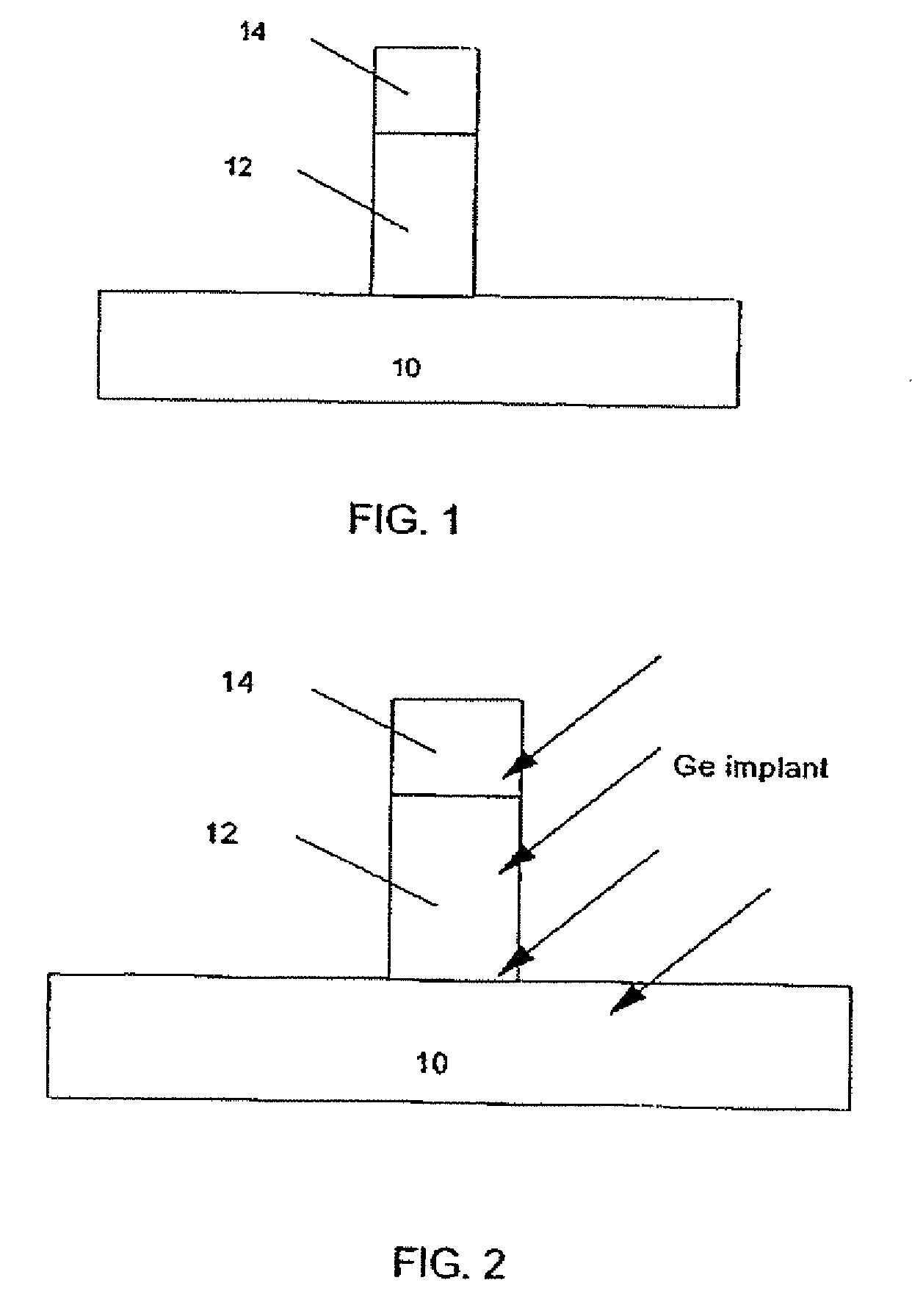
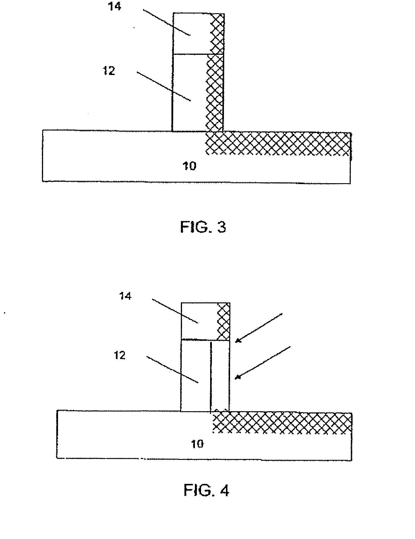
[0015] The invention relates to a semiconductor structure and method of manufacturing and more particularly to a FinFet device with a buried channel and a method of manufacturing. In one embodiment, the structure of the invention improves the mobility and hence significantly enhances operating frequency and performance of pMOSFETs. Additionally, by using the fabrication methods and hence achieving the final structure of the invention, it is also possible to more accurately gate control to the channel, as well as increase carrier mobility by keeping the carrier from a rough gate dielectric interface and control velocity overshoot close to the source. In one implementation, the thickness of a buried SiGe layer, in the channel, can be controlled through the fabrication process of the invention in order to achieve the beneficial affects of the invention.
[0016] Referring to FIG. 1, a starting structure is shown, which includes a Si fin 12 formed on a BOX 10 (buried oxide). A nitride har...
PUM
 Abstract
Description
Claims
Application Information
 - R&D Engineer
- R&D Manager
- IP Professional
- Industry Leading Data Capabilities
- Powerful AI technology
- Patent DNA Extraction
Browse by: Latest US Patents, China's latest patents, Technical Efficacy Thesaurus, Application Domain, Technology Topic, Popular Technical Reports.
© 2024 PatSnap. All rights reserved.Legal|Privacy policy|Modern Slavery Act Transparency Statement|Sitemap|About US| Contact US: help@patsnap.com