Process for electroless copper deposition

a technology of electroless copper and deposition layer, which is applied in the direction of liquid/solution decomposition chemical coating, solid-state device, coating, etc., can solve the problems of copper diffusion into neighboring layers, electronic devices to fail, and dielectric layers to become conductiv

Inactive Publication Date: 2007-05-03
APPLIED MATERIALS INC
View PDF99 Cites 142 Cited by
  • Summary
  • Abstract
  • Description
  • Claims
  • Application Information

AI Technical Summary

Benefits of technology

[0016] In another embodiment, a method for forming a copper-containing material on a substrate is provided that includes forming a barrier layer having a thickness of about 20 Å or less on a substrate during an ALD process or a PVD process, forming a ruthenium layer having a thickness of about 20 Å or less on the barrier layer during an ALD process or PVD process and exposing the substrate to an electroless copper solution to form a copper material on the ruthenium layer. In one example, the barrier layer contains a tantalum nitride layer deposited on a tantalum layer.

Problems solved by technology

Although copper is a popular interconnect material, devices containing copper materials may also suffer since copper by diffuse into neighboring layers, such as dielectric layers.
The resulting and undesirable presence of copper causes dielectric layers to become conductive and electronic devices to fail.
Tantalum nitride does have some negative characteristics, which include poor adhesion to the copper layer deposited thereon.
Poor adhesion of the subsequently deposited copper layers can lead to poor electromigration in the formed device and possibly cause process contamination issues in subsequent processing steps, such as during a chemical mechanical polishing (CMP) process.

Method used


Image

  • Process for electroless copper deposition
  • Process for electroless copper deposition

Examples


example 1

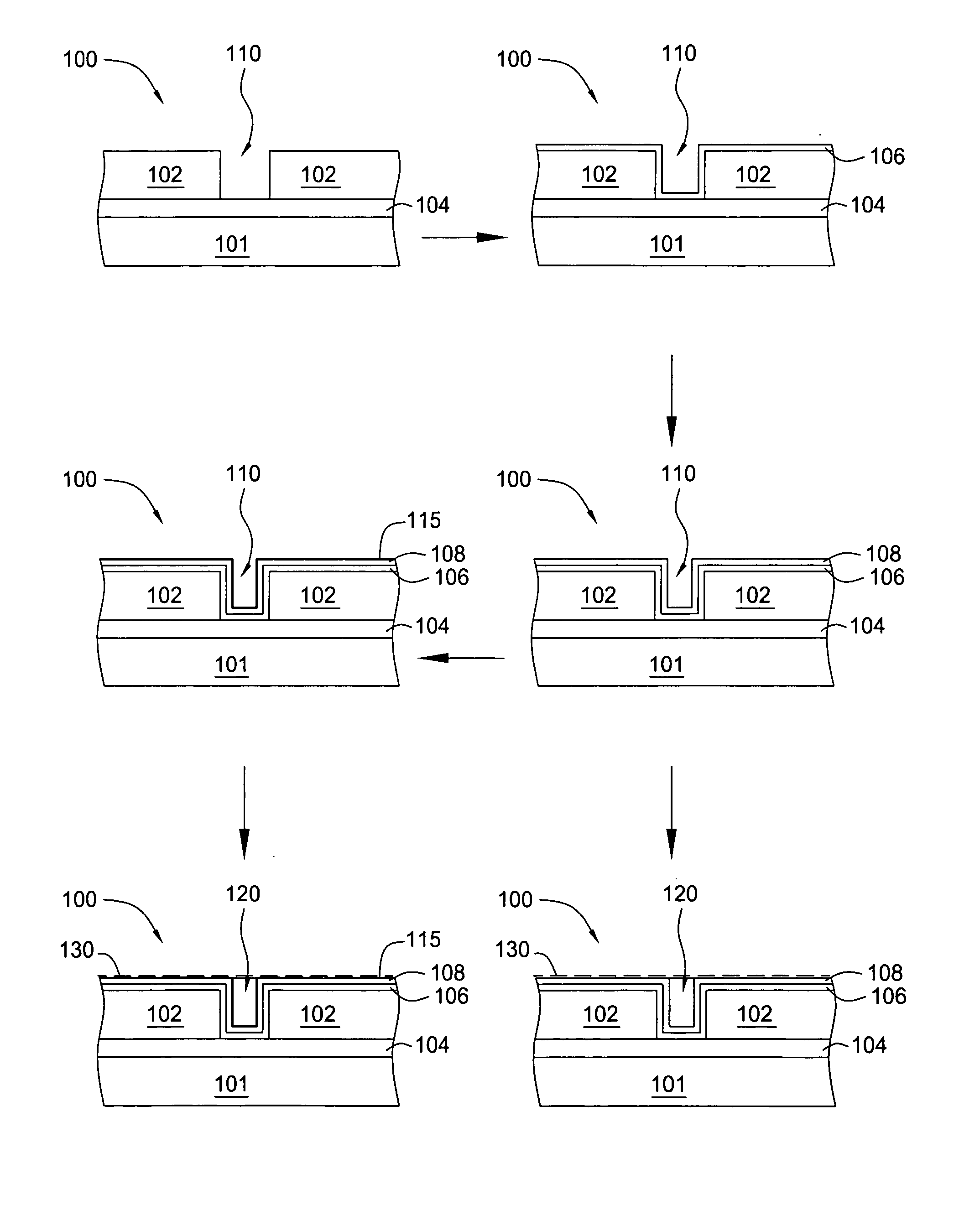
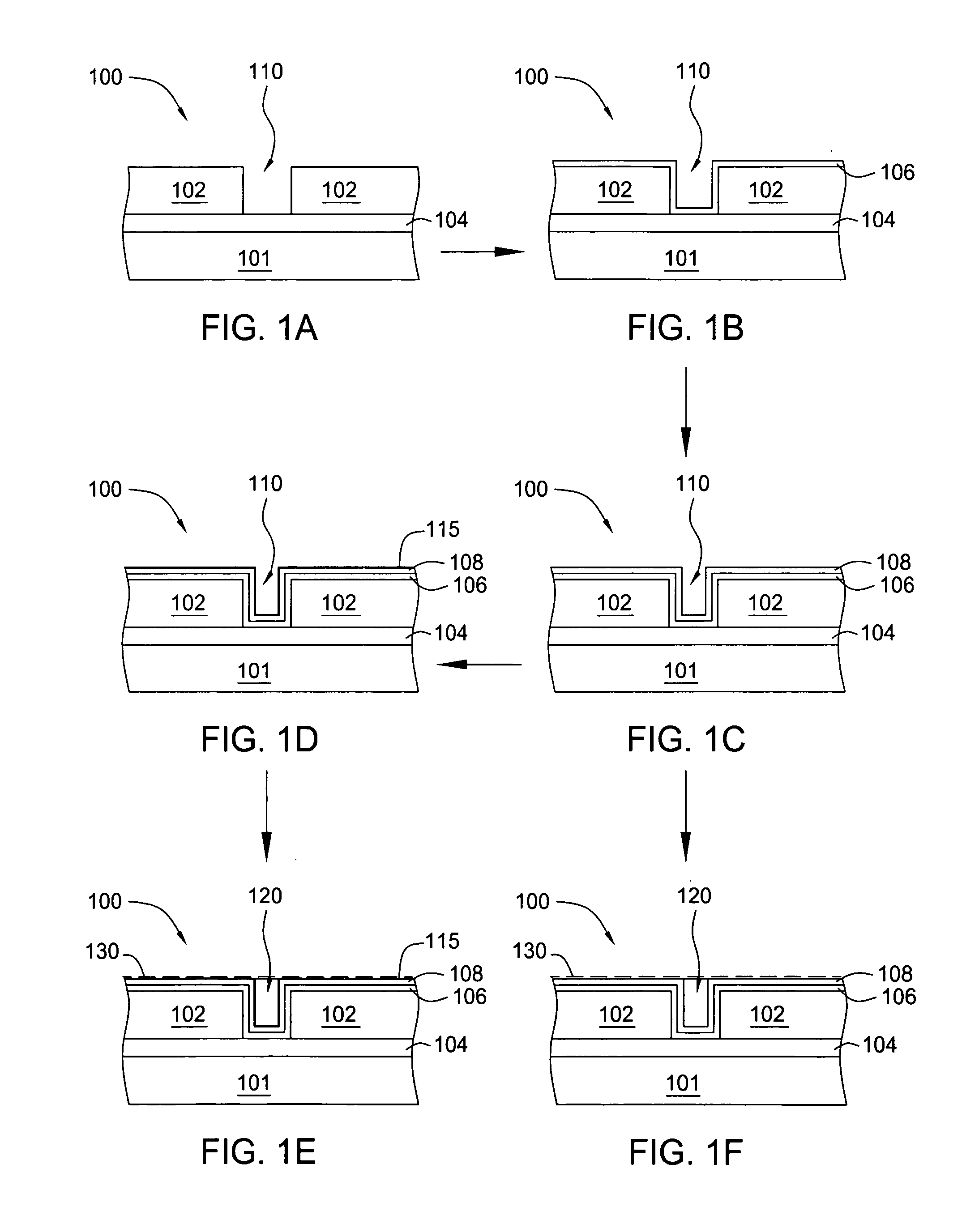
[0054] The subsequent steps follow: a) deposition of a barrier layer (e.g., ALD or PVD of tantalum nitride); b) deposition of ruthenium layer by ALD or PVD; c) expose substrate to annealing process; d) deposition of seed copper by electroless, ECP or PVD; and e) deposition of bulk copper by electroless or ECP.

example 2

[0055] The subsequent steps follow: a) pre-clean of the substrate; b) deposition of a barrier layer (e.g., ALD or PVD of tantalum nitride); c) deposition of ruthenium layer by ALD or PVD; d) deposition of seed copper by electroless, ECP or PVD; and e) deposition of bulk copper by electroless or ECP.

example 3

[0056] The subsequent steps follow: a) deposition of a barrier layer (e.g., ALD or PVD of tantalum nitride); b) punch-thru step; c) deposition of ruthenium layer by ALD or PVD; d) deposition of seed copper by electroless, ECP or PVD; and e) deposition of bulk copper by electroless or ECP.


PUM

PropertyMeasurementUnit
concentrationaaaaaaaaaa
pressureaaaaaaaaaa

Abstract

Embodiments of the invention provide a method for depositing a copper material on a substrate by an electroless deposition process and also provide a composition of an electroless deposition solution. In one embodiment, the copper material is deposited from an electroless copper solution that contains an additive, such as an inhibitor, to promote a bottom-up fill process. In one aspect, the field of the substrate may be maintained free of copper material or substantially free of copper material during the electroless deposition process. Prior to the electroless deposition process for forming the copper material, a barrier layer may be deposited on the substrate, and thereafter, a ruthenium layer may be deposited thereon. In one example, the copper material is formed during a bottom-up, electroless deposition process directly on the ruthenium layer. Alternatively, a seed layer may be formed on the ruthenium layer prior to depositing the copper material.

Description

BACKGROUND OF THE INVENTION [0001] 1. Field of the Invention [0002] Embodiments of the invention generally relate to a method for depositing materials on a substrate, and more particularly to methods for forming a copper material on a substrate surface by an electroless deposition process. [0003] 2. Description of the Related Art [0004] Multilevel metallization for nodes of 45 nm, 32 nm or smaller is an important technology for the next generation of very large scale integration (VLSI). The multilevel interconnects that lie at the heart of this technology include high aspect ratio features, such as contacts, vias, lines and other apertures. Reliable formation of these features is important for the success of VLSI and the continued effort to increase quality and circuit density on individual substrates. Therefore, there is a great amount of ongoing effort being directed to the formation of void-free features having high aspect ratios of 10:1 (height:width) or greater. [0005] Copper i...

Claims


Application Information

Patent Timeline
Patent Type & Authority Applications(United States)
IPC IPC(8): H01L21/44
CPCC23C18/165C23C18/40C25D3/38H01L21/288H01L21/76844H01L21/76846H01L21/76862H01L21/76864H01L21/76874H01L21/76879H01L2221/1089
Inventor WIJEKOON, KAPILAWEIDMAN, TIMOTHY W.SHANMUGASUNDRAM, ARULKUMAR
Owner APPLIED MATERIALS INC
Why Eureka
Try Eureka