

Reduction of mechanical stress on pattern specific geometries during etch using double pattern layout and process approach
a technology of mechanical stress and pattern specific geometries, applied in the field of semiconductor devices, can solve the problems of lithographic distortion, structural errors of hard masks, and the critical dimension (cd) of their corresponding mask pattern approaching the resolution limit of optical exposure tools, so as to reduce the width
- Summary
- Abstract
- Description
- Claims
- Application Information
AI Technical Summary
Benefits of technology
Problems solved by technology
Method used
Image

Examples
Embodiment Construction
[0001] 1. Field of the Invention
[0002] The present invention relates to semiconductor devices and methods for their fabrication. More particularly, the present invention relates to methods for reducing errors in a patterned mask due to mechanical stress during fabrication of semiconductor devices.
[0003] 2. Background of the Invention
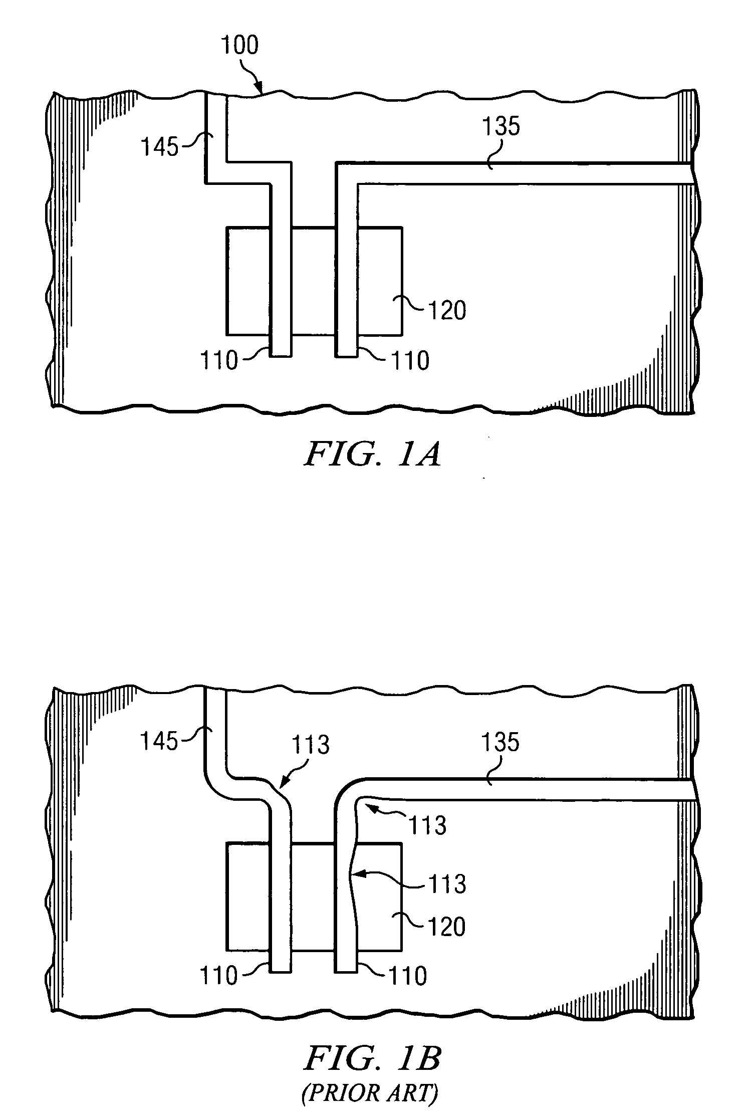
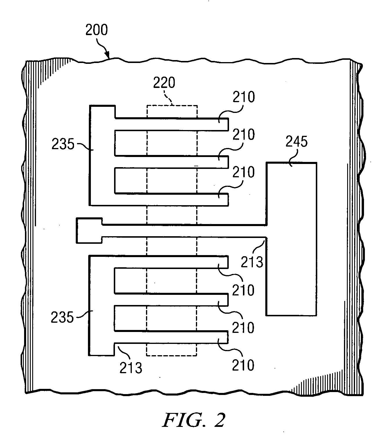
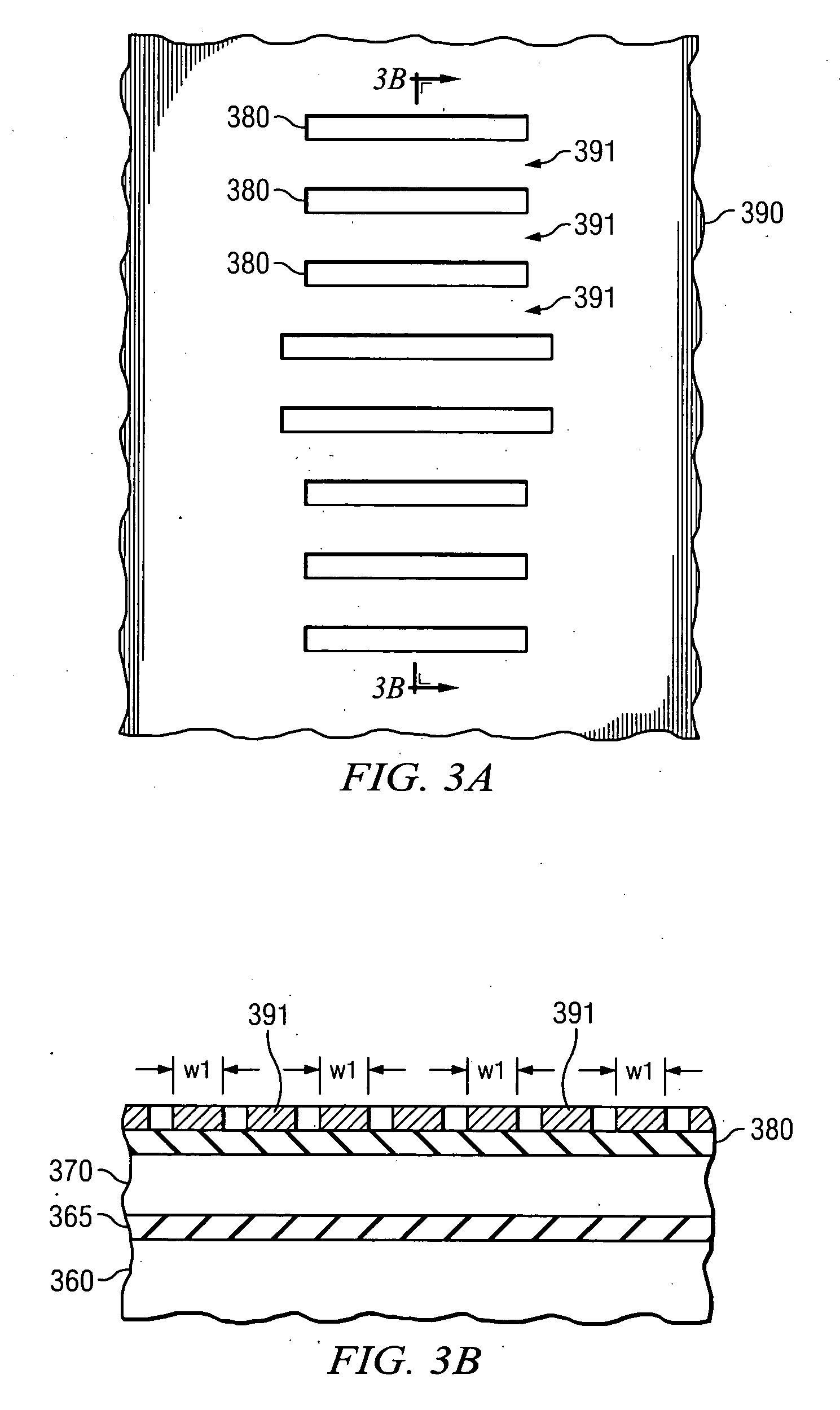
[0004] Lithographic projection apparatus (tools) can be used, for example, in the manufacture of integrated circuits (ICs). When using the various tools, a mask can be used that contains a circuit pattern corresponding to an individual layer of the IC, and this pattern can be imaged onto a target portion (e.g., comprising one or more dies) on a substrate, such as a silicon or other wafer comprising a semiconductor, that has been coated with a layer of radiation-sensitive material, such as a resist.
[0005] The masks comprise geometric patterns corresponding to the circuit components to be integrated onto a substrate. The patterns used to create such ma...
PUM
| Property | Measurement | Unit |
|---|---|---|
| width | aaaaa | aaaaa |
| size | aaaaa | aaaaa |
| width W1 | aaaaa | aaaaa |
Abstract
Description
Claims
Application Information