

Method of forming oxide film of semiconductor device
a semiconductor device and oxide film technology, applied in the field of semiconductor devices, can solve the problems of degrading the properties of the tunnel oxide film, unsuitable methods, and degrading the properties, and achieve the effect of preventing the coherence of nitrogen
- Summary
- Abstract
- Description
- Claims
- Application Information
AI Technical Summary
Benefits of technology
Problems solved by technology
Method used
Image

Examples
Embodiment Construction
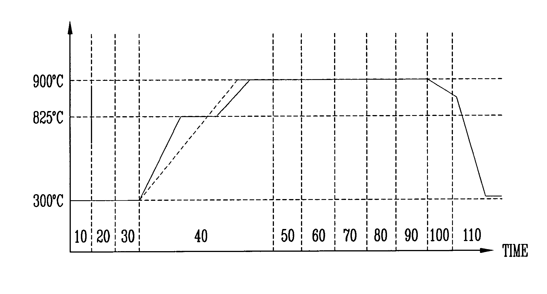
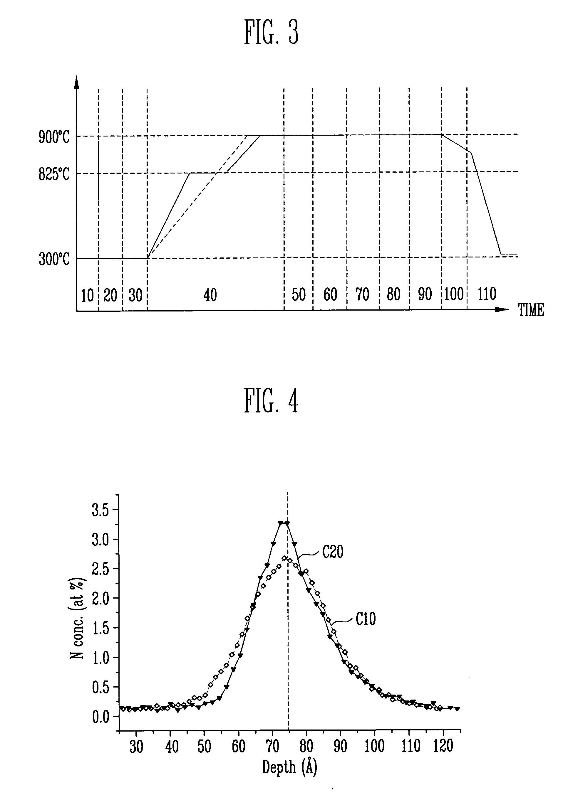
[0021] Referring to FIG. 3,a semiconductor substrate in which predetermined structures (e.g., wells) are already formed is loaded onto a boat. The boat is then loaded into the radical oxidization apparatus (step 10). Upon loading, a small amount of oxygen (e.g., ˜1%) is introduced and the radical oxidization apparatus is maintained at a temperature of 300 to 600° C.
[0022] After the boat is loaded, the radical oxidization apparatus is stabilized for a predetermined time (step 20). At this time, the boat is rotated in order to improve the thickness uniformity. The boat is rotated at a rate of about 1 to 2 rpm. Furthermore, when the boat is loaded, the apparatus is kept in an ozone environment in order to remove organic contaminants adsorbed on the top surface of the semiconductor substrate. The ozone is kept to a density of 100 to 200 g / N m3 (grams per normal cubic meter).
[0023] The vacuum in the radical oxidization apparatus is maintained for a time period (step 30). This is for th...
PUM
 Abstract
Description
Claims
Application Information