Image sensor and fabricating method thereof

Inactive Publication Date: 2007-05-10
DONGBU ELECTRONICS CO LTD
View PDF7 Cites 21 Cited by
  • Summary
  • Abstract
  • Description
  • Claims
  • Application Information

AI Technical Summary

Benefits of technology

[0032] The present invention provides an image sensor and fabricating method thereof, by which total photoelectric

Problems solved by technology

However, the conventional image sensor and fabricating method thereof have at least the following problem.
Thus, if the flowing pr

Method used


Image

  • Image sensor and fabricating method thereof
  • Image sensor and fabricating method thereof
  • Image sensor and fabricating method thereof

Examples


Embodiment Construction

[0054] Reference will now be made in detail to the preferred embodiments of the present invention, examples of which are illustrated in the accompanying drawings. Wherever possible, the same reference numbers will be used throughout the drawings to refer to the same or like parts.

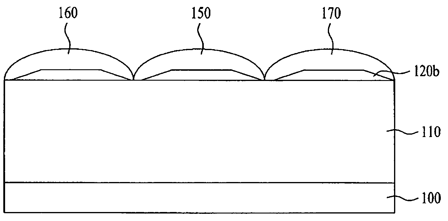
[0055]FIG. 4 is a cross-sectional diagram of an image sensor according to the present invention.

[0056] Referring to FIG. 4, an image sensor according to the present invention includes a substrate 100; a sublayer 110 on the substrate 100 to include a photodiode, various transistors and metal lines; a plurality of pattern layers 120b on the sublayer 110 overlapped with the photodiode to have curved surfaces, respectively; and R, G and B color filter layers 150, 160 and 170 regularly arranged on a prescribed area of the pattern layers 120b along the curved surfaces of the pattern layers 120b, respectively. In this case, the pattern layers 120b are spaced apart from each other to leave 0.5-1 μm spacing betwee...


PUM


Abstract

An image sensor includes the steps of forming a sublayer including a photodiode, a transistor and a metal line on a substrate, forming a pattern layer on the sublayer to be overlapped with the photodiode and to having a curved surface, and forming a combined color filter and microlens on the pattern layer to have a curved surface.

Description

CROSS-REFERENCE TO RELATED APPLICATION [0001] This application claims the benefit of Korean Patent Application No. 10-2005-0107682, filed on Nov. 10, 2005, which is hereby incorporated by reference as if fully set forth herein. BACKGROUND OF THE INVENTION [0002] 1. Field of the Invention [0003] The present invention relates to a semiconductor device, and more particularly, to an image sensor and fabricating method thereof. Although the present invention is suitable for a wide scope of applications, it is particularly suitable for enabling total photoelectric conversion without light loss by enhancing the surface uniformity of a microlens in each area. [0004] 2. Discussion of the Related Art [0005] Generally, an image sensor is a semiconductor device that converts an optical image to an electric signal. And, image sensors are mainly classified into a charge coupled device (CCD) or a complementary metal oxide silicon (CMOS) image sensor. [0006] The image sensor includes a photodiode u...

Claims


Application Information

Patent Timeline
IPC IPC(8): H01L27/00
CPCH01L27/14627H01L27/14685H01L27/146
Inventor KIM, SANG SIK
Owner DONGBU ELECTRONICS CO LTD
Why Eureka
Try Eureka