CMOS image sensor

a sensor and image technology, applied in the field of image sensors, can solve the problems of narrow dynamic range, undesirable image lag, narrow dynamic range, etc., and achieve the effects of reducing clock feedthrough, image lag, and improving dynamic rang

Active Publication Date: 2007-05-10
SK HYNIX INC
View PDF8 Cites 16 Cited by
  • Summary
  • Abstract
  • Description
  • Claims
  • Application Information

AI Technical Summary

Benefits of technology

[0011] It is one object of the present invention to provide an improved CMOS image sensor integrated with a pinned photodiode, which is capable of reducing clock feedthrough, image lag, and improving dynamic range.

Problems solved by technology

CMOS sensors typically suffer from narrow dynamic range and poor charge transfer efficiency.
If the distance “B” is too small, pinch-off occurs resulting in narrow dynamic range and undesirable image lags.
However, the prior art non-self-aligned method suffers from so-called fixed pattern noise due to misalignment of the lithography and non-uniformity of the overlapping portion “A” among pixels.
On the other hand, the above-described prior art CMOS sensor has another drawback in that a potential “pocket” indicated by numeral number 50 forms due to an excessively large overlapping portion “A”.
The potential “pocket”50 is caused by a large number of trapped electrons accumulated underneath the gate 30, which leads to deteriorated clock feed-through of the gate 30 of the transfer transistor, image lag, and also poor dynamic range.

Method used


Image

  • CMOS image sensor
  • CMOS image sensor
  • CMOS image sensor

Examples


Embodiment Construction

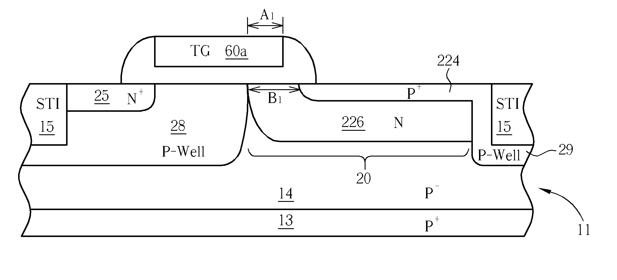
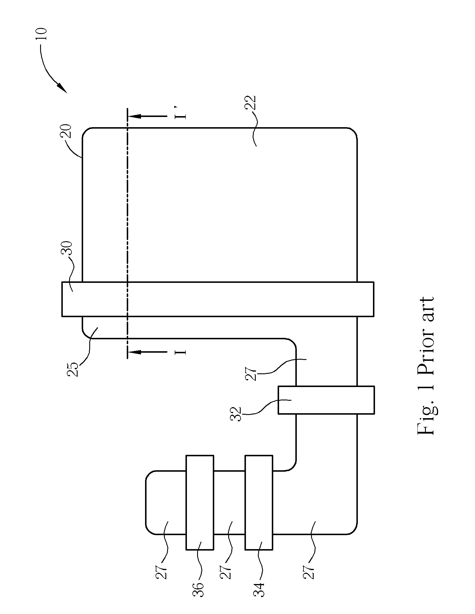
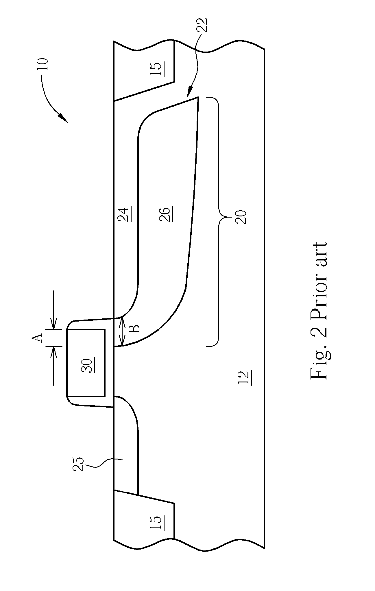
[0023] Please refer to FIGS. 4-6. FIG. 4 is a top view of an exemplary four-transistor (4T) pixel cell of a CMOS sensor 100 according to one preferred embodiment of this invention; and FIGS. 5 and 6 are schematic, cross-sectional diagrams taken along line 11-11′ and line III-III′ of FIG. 4, respectively, where like numeral numbers designate like elements, regions or layers.

[0024] As shown in FIG. 4, the CMOS sensor 100 comprises a charge-accumulating region 20 in an underlying portion of a substrate 11. A pinned photodiode 220 is formed in the charge-accumulating region 20. A transfer gate 60 is provided for transferring photoelectric charges generated in the charge-accumulating region 20 to a floating diffusion region (sensing node) 25.

[0025] The floating diffusion region 25 is coupled to a gate 34 of a source follower transistor. The source follower transistor provides an output signal to a row select access transistor having a gate 36. A reset transistor having a gate 32 resets...


PUM


Abstract

A CMOS image sensor includes a semiconductor substrate; a pinned photodiode formed in a light-sensing region of the semiconductor substrate, the pinned photodiode comprising a charge-accumulating diffusion region and a surface pinning diffusion region overlying the charge-accumulating diffusion region; a transfer transistor, wherein the transfer transistor has a transfer gate comprising a protruding first gate segment with a first gate dimension and a second gate segment with a second gate dimension that is smaller than the first gate dimension. A first overlapping portion between the protruding first gate segment and the charge-accumulating diffusion region is greater than a second overlapping portion between the second gate segment and the charge-accumulating diffusion region.

Description

BACKGROUND OF THE INVENTION [0001] 1. Field of the Invention [0002] The present invention relates to an image sensor and, more particularly, to a CMOS image sensor integrated with a pinned photodiode, which is capable of reducing clock feedthrough and improving dynamic range. [0003] 2. Description of the Prior Art [0004] CMOS (complementary metal-oxide-semiconductor) image sensor or CMOS sensor is known in the art. Generally, a CMOS sensor includes a plurality of unit pixels having a light-sensing region and a peripheral circuit region. Each of the unit pixels also includes a light-sensing element such as a photodiode formed in the light-sensing region and a plurality of transistors formed on the peripheral circuit region. The photodiode senses incident light and accumulates image charges that are generated due to the incident light. [0005]FIG. 1 illustrates a layout of four-transistor (4T) pixel cell 10 of a conventional CMOS sensor. FIG. 2 is a schematic, cross-sectional view of t...

Claims


Application Information

Patent Timeline
Patent Type & Authority Applications(United States)
IPC IPC(8): H01L31/113
CPCH01L27/14603H01L27/14641H01L27/14643
Inventor CHEN, CHING-WEIHSIEH, CHIH-CHENGHUANG, CHIEN-CHANG
Owner SK HYNIX INC
Why Eureka
Try Eureka