Differential mechanical stress-producing regions for integrated circuit field effect transistors

a technology of field effect transistors and mechanical stress, which is applied in the direction of electrical equipment, semiconductor devices, radio frequency controlled devices, etc., can solve the problems of affecting the performance of the device, so as to achieve the effect of sufficient material stress

Active Publication Date: 2007-05-10
CHARTERED SEMICONDUCTOR MANUFACTURING +1
View PDF8 Cites 3 Cited by
  • Summary
  • Abstract
  • Description
  • Claims
  • Application Information

AI Technical Summary

Benefits of technology

[0006] Field effect transistors according to some embodiments of the present invention include a substrate, an isolation region in the substrate that defines an active region in the substrate, spaced apart source / drain regions in the active region, a channel region in the active region between the spaced apart source / drain regions and an insulated gate on the channel region. A differential mechanical stress-producing region is provided that is configured to produce different mechanical stress in the channel region adjacent the isolation region, compared to remote from the isolation region. In some embodiments, the differential material stress is sufficient to reduce, and in some embodiments prevent, turn-on of the channel region adjacent the isolation region prior to turn-on of the channel region remote from the isolation region. In some embodiments, the differential mechanical stress-producing region comprises a patterned stress management film. In other embodiments, the differential mechanical stress-producing region comprises a patterned stress-producing implant. In other embodiments, the differential mechanical stress-producing region comprises a patterned silicide film. Accordingly, a channel region of a field effect transistor has different mechanical stress therein adjacent the isolation region compared to remote from the isolation region.
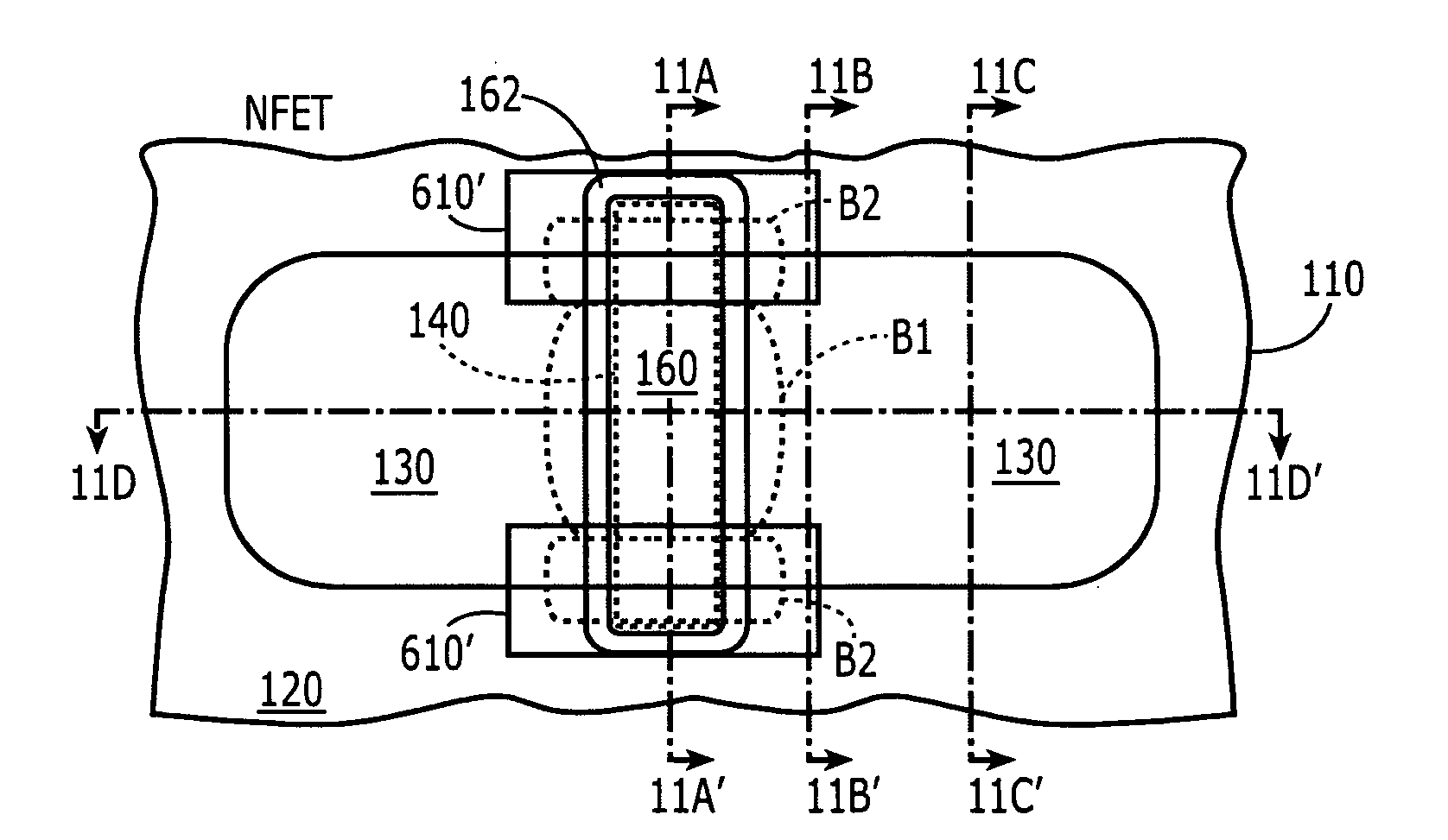
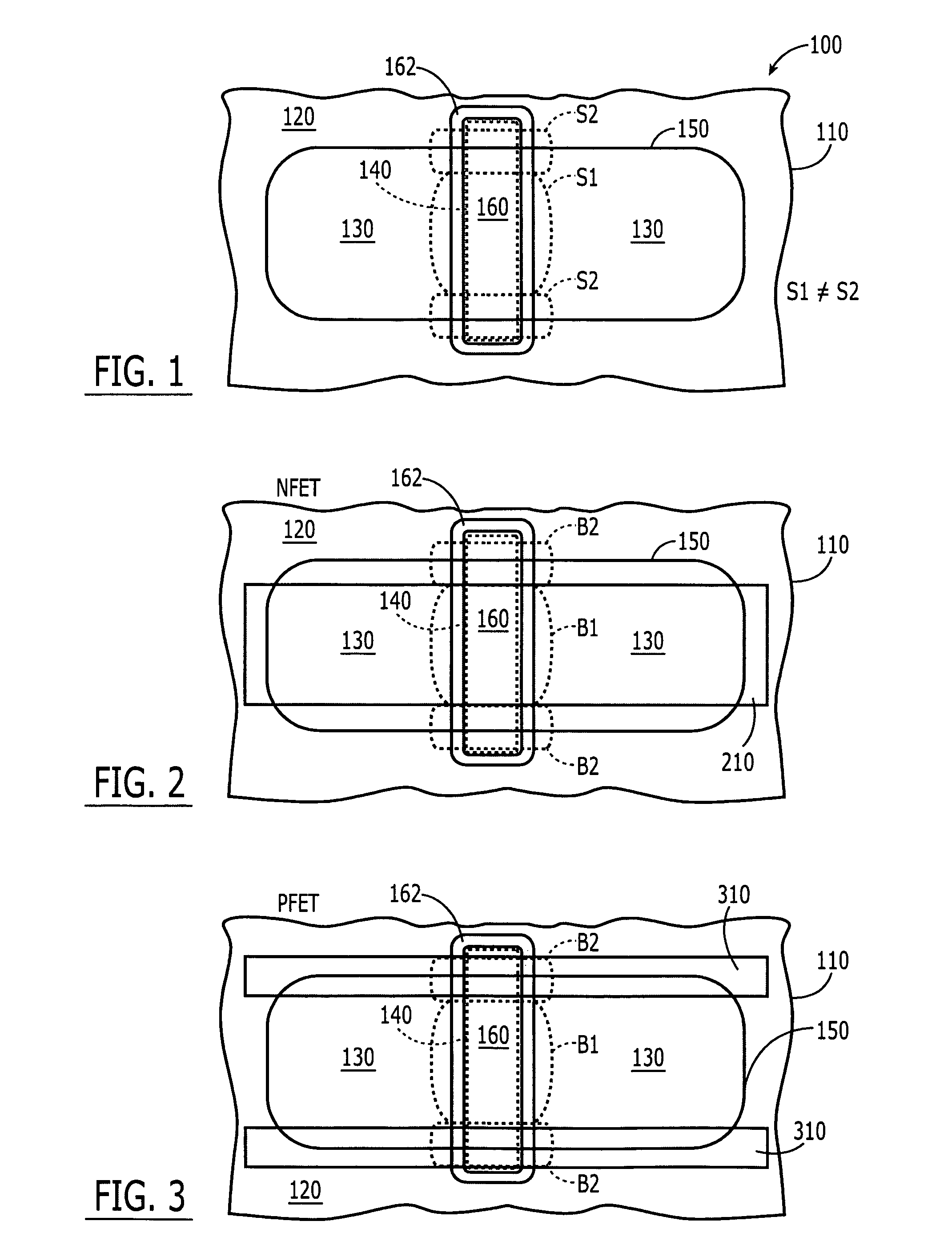
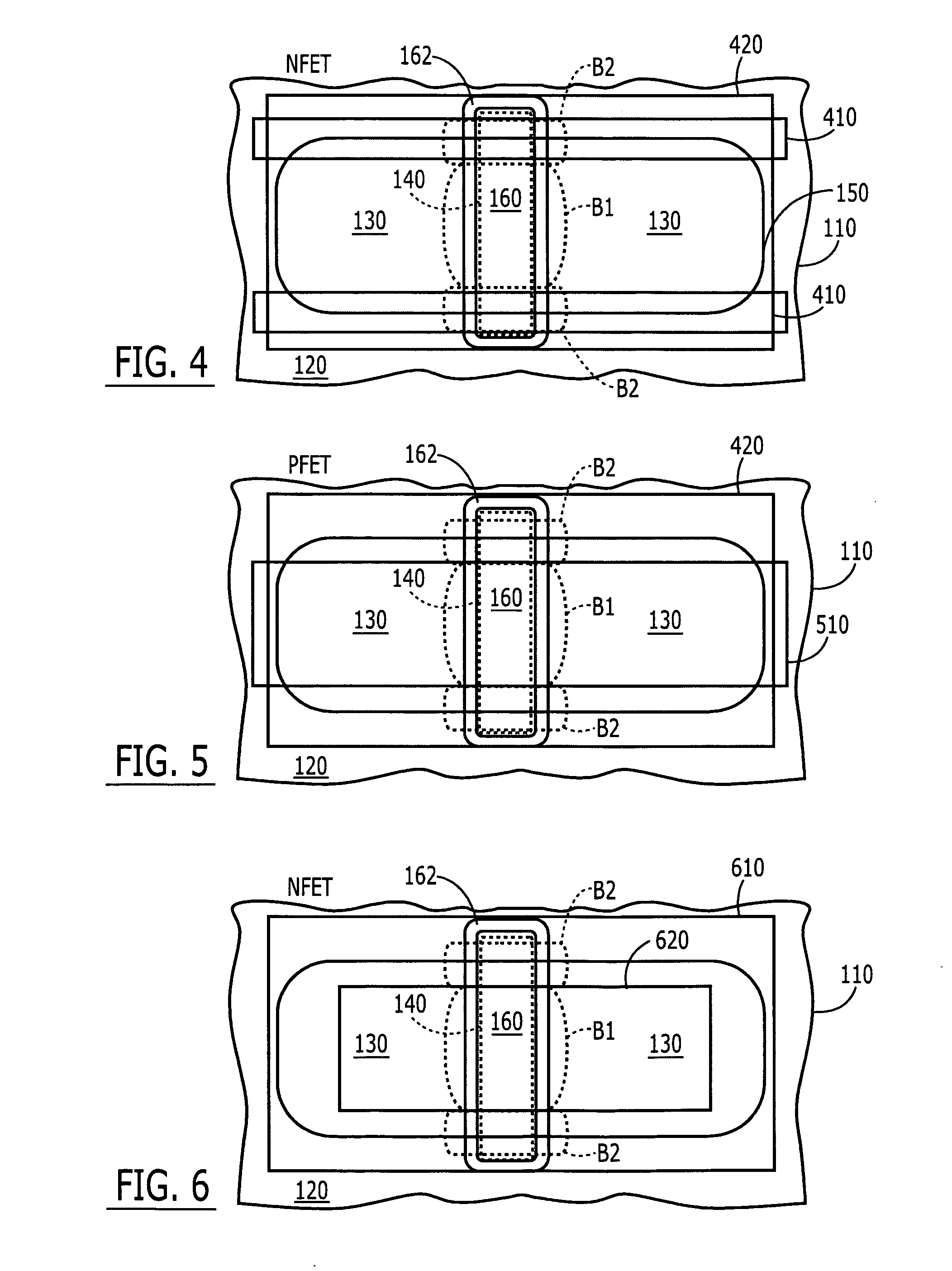
[0007] Embodiments of the invention that use a stress management film to provide a differential stress-producing region can be used with both N-channel and P-channel field effect transistors. In particular, when the field effect transistor is an N-channel field effect transistor, the patterned stress management film is present at a first boundary of the source / drain regions and the channel region that is remote from the isolation region, and is absent from a second boundary of the source / drain regions and the channel region that is adjacent the isolation region. When the field effect transistor is a P-channel field effect transistor, the patterned stress management film is absent from a first boundary of the source / drain regions and the channel region that is remote from the isolation region and is present at a second boundary of the source / drain regions and the channel region that is adjacent the isolation region.
[0008] Patterned stress-producing implants also may be used to produce the differential mechanical stress-producing region according to some embodiments of the present invention, for both N-channel and P-channel field effect transistors. In particular, when the field effect transistor is an N-channel field effect transistor, the patterned stress-producing implant is absent at a first boundary of the source / drain regions and the channel region that is remote from the isolation region and is present at a second boundary of the source / drain regions and the channel region that is adjacent the isolation region. When the field effect transistor is a P-channel field effect transistor, the patterned stress-producing implant is present at a first boundary of the source / drain regions and the channel region that is remote from the isolation region and is absent from a second boundary of the source / drain regions and the channel region that is adjacent the isolation region.
[0009] When the differential mechanical stress-producing region comprises a patterned silicide film, the patterned silicide film may be used in both N-channel and P-channel field effect transistors. In particular, when the field effect transistor is an N-channel field effect transistor, the patterned silicide film is present at a first boundary of the source / drain regions and the channel region that is remote from the isolation region, and is absent from a second boundary of the source / drain regions and the channel region that is adjacent the isolation region. In some embodiments, a patterned silicide blocking film is provided on the substrate that is present at the second boundary and is absent from the first boundary. In other embodiments, a patterned gate sidewall spacer is provided on the substrate that is present at the second boundary and is absent from the first boundary. When the field effect transistor is a P-channel field effect transistor, the patterned silicide film is absent from the first boundary and is present on the second boundary. In some embodiments, this presence and absence of the silicide film is provided by a patterned silicide blocking film that is absent from the second boundary and is present at the first boundary. In other embodiments, this presence and absence of the silicide film is provided by a patterned gate sidewall spacer on the substrate that is absent from the second boundary and is present at the first boundary. In all of these embodiments, the silicide film may also be present on the gate electrode at the first boundary and at the second boundary.
[0010] Analogous methods of fabricating a field effect transistor may be provided according to various embodiments of the present invention, wherein an isolation region, an active region, spaced apart source / drain regions, a channel region and an insulated gate may be formed conventionally. A differential mechanical stress-producing region is formed in and / or on the substrate that is configured to produce differential mechanical stress in the channel region adjacent the isolation region compared to remote from the isolation region. Stress management films may be patterned, stress-producing ions may be implanted and / or a silicide film may be patterned, as was described above, to provide various embodiments of differential mechanical stress-producing regions.

Problems solved by technology

As the integration density of integrated circuit devices continues to increase, effects may be produced that can degrade the performance of the integrated circuit transistors.
As the integration density of integrated circuit field effect transistors continues to increase, undesirable effects may originate at the corner of the device, i.e., in the channel region under the insulated gate near the isolation regions.
The lower threshold voltage may provide a parallel path for current conduction, which has different turn-on characteristics, and may adversely affect the performance of the device.
It is also known that the silicide contacts may produce unwanted effects adjacent the isolation region.

Method used


Image

  • Differential mechanical stress-producing regions for integrated circuit field effect transistors
  • Differential mechanical stress-producing regions for integrated circuit field effect transistors
  • Differential mechanical stress-producing regions for integrated circuit field effect transistors

Examples


Embodiment Construction

[0014] The invention will be described more fully hereinafter with reference to the accompanying drawings, in which example embodiments of the invention are shown. This invention may, however, be embodied in many different forms and should not be construed as limited to the example embodiments set forth herein. Rather, the disclosed embodiments are provided so that this disclosure will be thorough and complete, and will fully convey the scope of the invention to those skilled in the art. In the drawings, the size and relative sizes of layers and regions may be exaggerated for clarity. Moreover, each embodiment described and illustrated herein includes its complementary conductivity type embodiment as well. Like numbers refer to like elements throughout.

[0015] It will be understood that when an element or layer is referred to as being “on”, “connected to” and / or “coupled to” another element or layer, it can be directly on, connected or coupled to the other element or layer or interv...


PUM


Abstract

Integrated circuit field effect transistors include a substrate, an isolation region in the substrate that defines an active region in the substrate, spaced apart source/drain regions in the active region, a channel region in the active region between the spaced apart source/drain regions and an insulated gate on the channel region. A differential mechanical stress-producing region is configured to produce different mechanical stress in the channel region adjacent the isolation region compared to remote from the isolation region. The differential mechanical stress-producing region may be formed using patterned stress management films, patterned stress-changing implants and/or patterned silicide films, and can reduce undesired comer effects. Related fabrication methods also are described.

Description

FIELD OF THE INVENTION [0001] This invention relates to integrated circuit devices and fabrication methods, and more particularly to integrated circuit field effect transistors and fabrication methods therefor. BACKGROUND OF THE INVENTION [0002] Integrated circuits are widely used for consumer, commercial and other applications. As is well known to those having skill in the art, an integrated circuit may include a large number of active devices, such as transistors, on an integrated circuit substrate. As the integration density of integrated circuit devices continues to increase, effects may be produced that can degrade the performance of the integrated circuit transistors. [0003] One widely used integrated circuit transistor is an integrated circuit field effect transistor. As is well known to those having skill in the art, an integrated circuit field effect transistor generally includes a substrate, such as a semiconductor substrate, and an isolation region, such as a shallow tren...

Claims


Application Information

Patent Timeline
Patent Type & Authority Applications(United States)
IPC IPC(8): H01L31/00
CPCH01L21/823412H01L21/823481H01L21/823807H01L21/823878H01L29/7842H01L29/7843H01L29/7847H01L29/665
Inventor SUN, MIN-CHULTEH, YOUNG WAY
Owner CHARTERED SEMICONDUCTOR MANUFACTURING
Why Eureka
Try Eureka