Eddy current sensor

a technology of eddy current and sensor, which is applied in the direction of electrical/magnetic thickness measurement, magnetic property measurement, instruments, etc., can solve the problems of adversely affecting the polishing performance of the chemical mechanical polishing apparatus, complicated and troublesome processes are required to measure the film thickness of the substrate, and achieve high accuracy and easy measurement

Active Publication Date: 2007-05-10
EBARA CORP
View PDF16 Cites 74 Cited by
  • Summary
  • Abstract
  • Description
  • Claims
  • Application Information

AI Technical Summary

Benefits of technology

[0008] The present invention has been made in view of the above drawbacks. It is, therefore, an object of the present invention to provide an eddy current sensor which is unlikely to be influenced from a measurement environment, and can readily measure a conductive film with high accuracy.
[0009] According to a first aspect of the present invention, there is provided an eddy current sensor having a sensor coil disposed near a conductive film formed on a substrate and a signal source configured to supply an AC signal to the sensor coil to produce an eddy current in the conductive film. The eddy current sensor includes a detection circuit operable to detect the eddy current produced in the conductive film. The detection circuit is connected to the sensor coil. The eddy current sensor also includes a housing made of a material having a high magnetic permeability. The housing accommodates the sensor coil therein. Thus, the housing is configured so that the sensor coil forms a path of a magnetic flux so as to effectively produce an eddy current in the conductive film.
[0010] With the above arrangement, a magnetic flux from the sensor coil forms a path (magnetic circuit) so as to pass through the housing having a high magnetic permeability, which is located around the sensor coil and then pass through the conductive film to be measured. Since the magnetic flux does not pass through a member in an installation environment, the magnetic flux is not attenuated. Thus, an eddy current can effectively be produced in the conductive film by the sensor coil, and the film thickness of the conductive film can be measured with high sensitivity.

Problems solved by technology

However, such formation of an opening may adversely affect polishing performance of the chemical mechanical polishing apparatus.
Accordingly, complicated and troublesome processes are required to measure the film thickness of the substrate.
Thus, complicated and troublesome processes are required to measure the film thickness of the substrate.

Method used


Image

  • Eddy current sensor
  • Eddy current sensor
  • Eddy current sensor

Examples


first embodiment

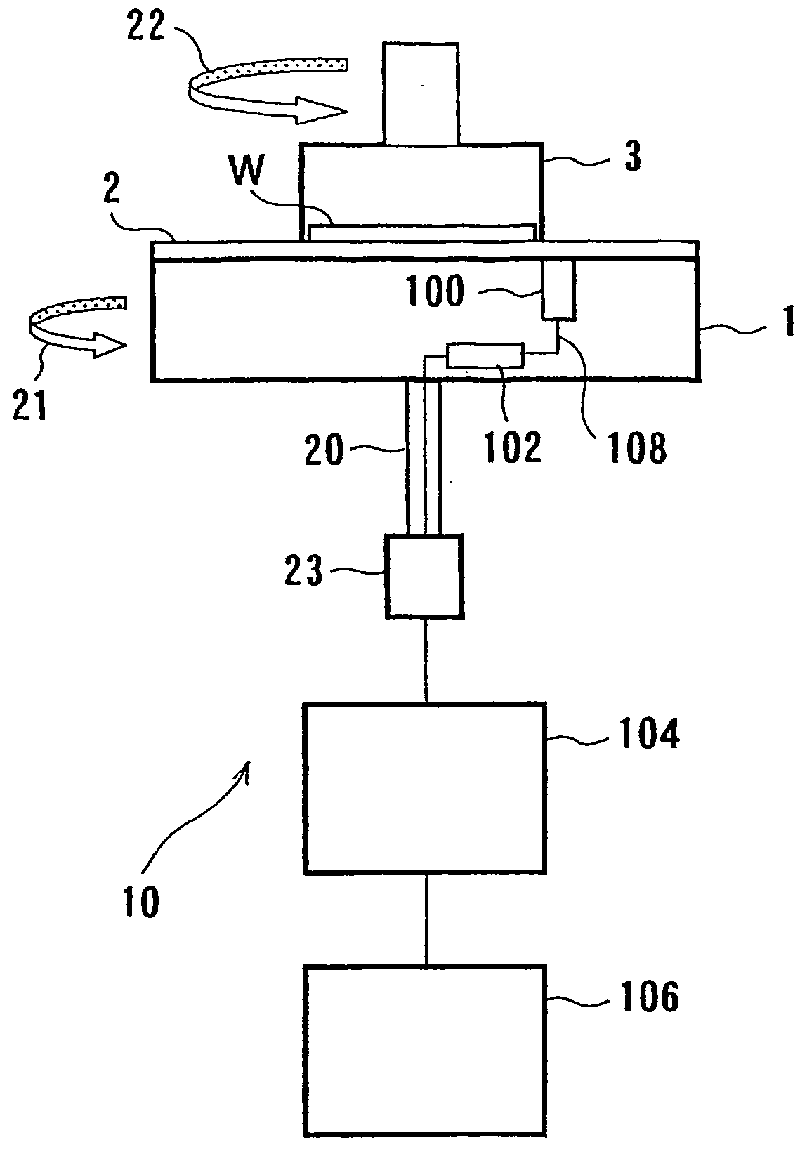
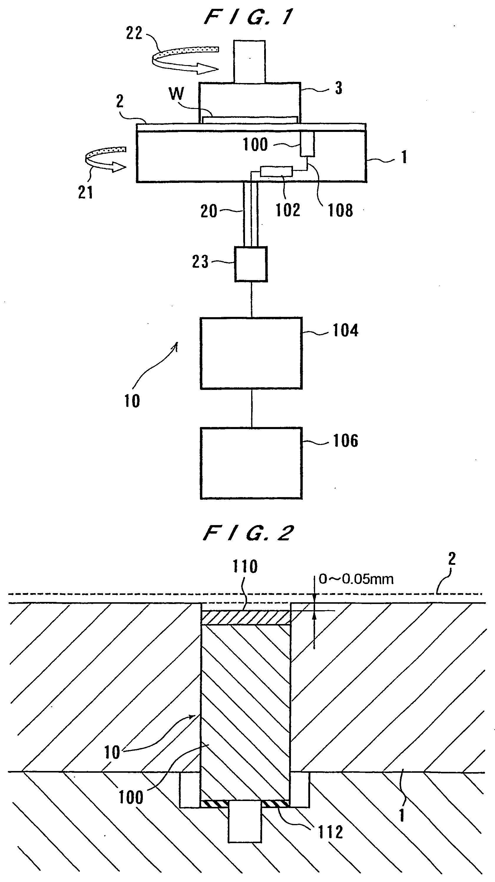
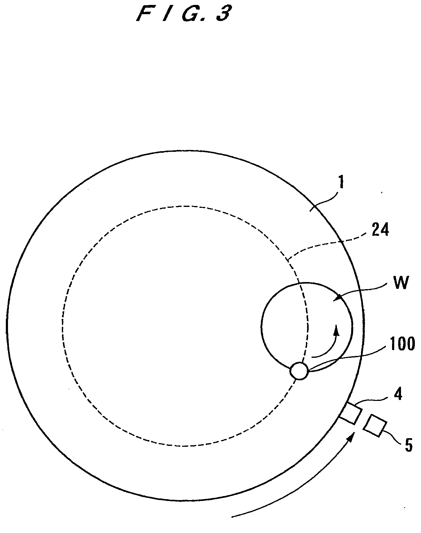
[0059]FIG. 1 shows a polishing apparatus having an eddy current sensor 10 according to the present invention. As shown in FIG. 1, the polishing apparatus has a polishing table 1, a polishing pad 2 attached to a surface of the polishing table 1, a top ring 3 for holding a semiconductor wafer W and pressing the semiconductor wafer W against the polishing pad 2, and an eddy current sensor 10 for measuring the film thickness of a conductive film, which is to be polished, on the semiconductor wafer W. The polishing table 1 of the polishing apparatus is rotatable about a support shaft 20 as shown by an arrow 21. The top ring 3 is rotatable about its axis as shown by an arrow 22.

[0060] The top ring 3 presses the semiconductor wafer W against the polishing pad 2 on the polishing table 1 while the top ring 3 and the polishing table 1 are rotated independently of each other. At that time, a polishing liquid is supplied onto the polishing pad 2 from a polishing liquid supply nozzle (not shown)...

second embodiment

[0138]FIG. 19 shows a sensor coil 100 according to the present invention. The sensor coil 100 is housed in a cylindrical housing 200 made of a material having a high magnetic permeability. As described above, when the polishing apparatus polishes the conductive film 6 of the semiconductor wafer W by the polishing pad, the sensor coil 100 is disposed in the polishing table 1 made of a conductive material such as a stainless material so as to measure the film thickness of the conductive film 6.

[0139] The housing 200 is made of a material having a high magnetic permeability, such as ferrite, amorphous material, permalloy, super-permalloy, or Mumetal. For example, the relative permeability μ of the housing 200 is 50. Thus, the housing 200 can pass a magnetic flux therethrough 50 times as much as air present around the sensor coil. In other words, the housing 200 can pass an equivalent magnetic flux with one-fiftieth thickness of an electrically insulating material such as a ceramic mate...


PUM


Abstract

An eddy current sensor (10) has a sensor coil (100) disposed near a conductive film (6) formed on a semiconductor wafer (W) and a signal source (124) configured to supply an AC signal to the sensor coil (100) to produce an eddy current in the conductive film (6). The eddy current sensor (10) includes a detection circuit operable to detect the eddy current produced in the conductive film (6). The detection circuit is connected to the sensor coil (100). The eddy current sensor (10) also includes a housing (200) made of a material having a high magnetic permeability. The housing (200) accommodates the sensor coil (100) therein. The housing (200) is configured so that the sensor coil (100) forms a path of a magnetic flux (MF) so as to effectively produce an eddy current in the conductive film (6).

Description

TECHNICAL FIELD [0001] The present invention relates to an eddy current sensor, and more particularly to an eddy current sensor suitable for detecting the thickness of a conductive film formed on a surface of a substrate such as a semiconductor wafer. The present invention also relates to a substrate processing apparatus, such as a polishing apparatus or a substrate deposition apparatus, having such an eddy current sensor. BACKGROUND ART [0002] In order to form interconnection circuits in a substrate such as a semiconductor wafer, there has been employed a process of plating a substrate with copper to form a copper layer thereon, and then removing unnecessary portions of the copper layer by chemical mechanical polishing (CMP) to form a copper interconnection layer in the substrate. During the chemical mechanical polishing (CMP) in such a process, it is necessary to accurately control the progress of the polishing process of the copper layer (the film thickness of the copper layer). ...

Claims


Application Information

Patent Timeline
Patent Type & Authority Applications(United States)
IPC IPC(8): G01B7/06G01B7/00H01L21/304
CPCG01B7/105G01N27/9006G01B7/02G01B7/06H01L21/02H01L21/304
Inventor TADA, MITSUOSUTO, YASUNARI
Owner EBARA CORP
Why Eureka
Try Eureka