Buffer circuit and use thereof

Inactive Publication Date: 2007-05-10
QIMONDA
View PDF5 Cites 0 Cited by
  • Summary
  • Abstract
  • Description
  • Claims
  • Application Information

AI Technical Summary

Benefits of technology

[0007] The configuration with elements having a diode-type transfer response at the terminals of the first transistor pair results in an increase in a breakdown voltage, so that the circuit is suitable even for applications having high input amplitudes. Moreover, the linearity of the transfer response is improved. By virtue of the second transistor pair, a linearity in the transfer characteristic curve is improved further and a higher driver capability is also achieved. At the same time, a parasitic capacitance of the circuit decreases as a result of the arrangement of the third transistor and the fourth transistor. As a result, the power consumption of the circuit is reduced and the efficiency and the current-carrying capacity are improved.

Problems solved by technology

Input signals having a high amplitude may, however, lead to a breakdown between the control terminal and the sink terminal of the transistors.
A particularly complicated and expensive process technology is thus required for high-voltage applications.
Undesired process fluctuations during the production of the individual transistors may adversely affect the changeover point of the output signal between a high and a low level, with the result that a changeover takes place at undesired values or the current consumption rises overall if both transistors are in the on state.

Method used


Image

  • Buffer circuit and use thereof
  • Buffer circuit and use thereof
  • Buffer circuit and use thereof

Examples


Embodiment Construction

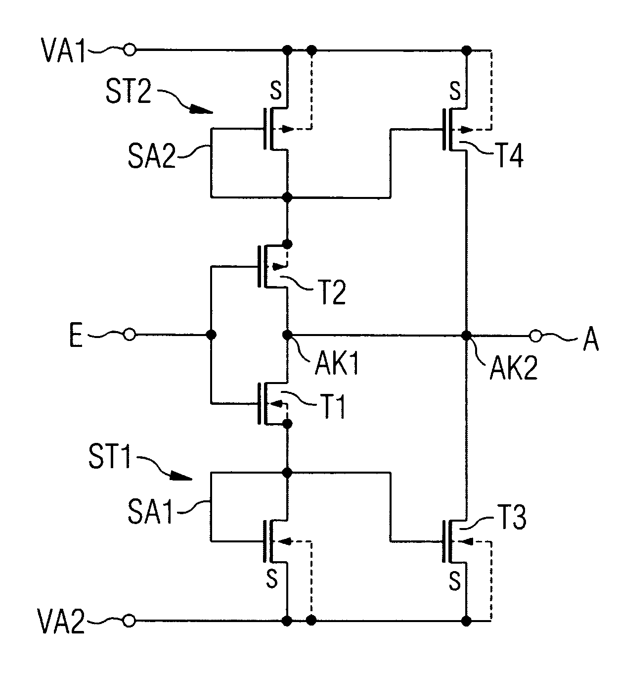
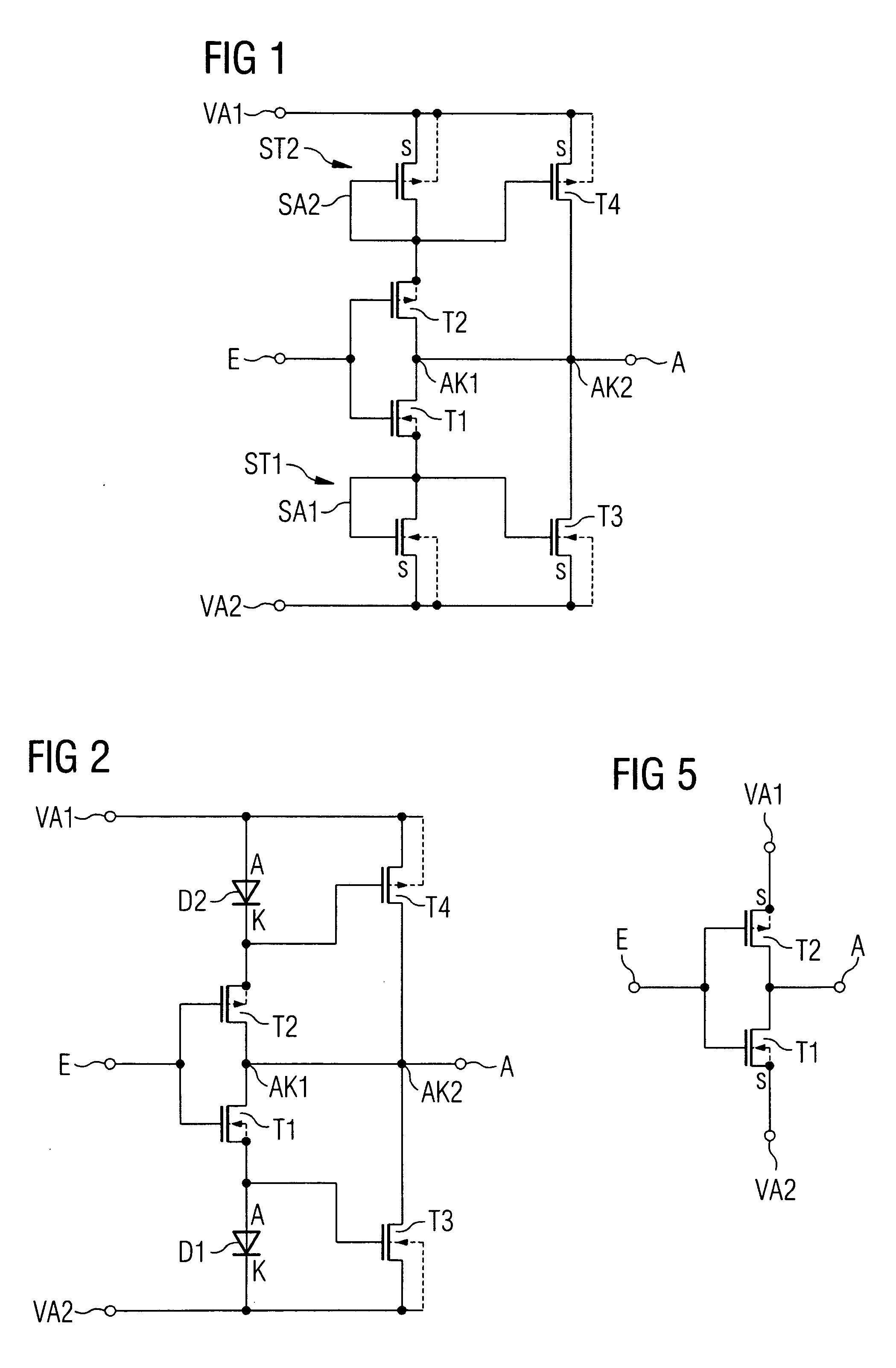
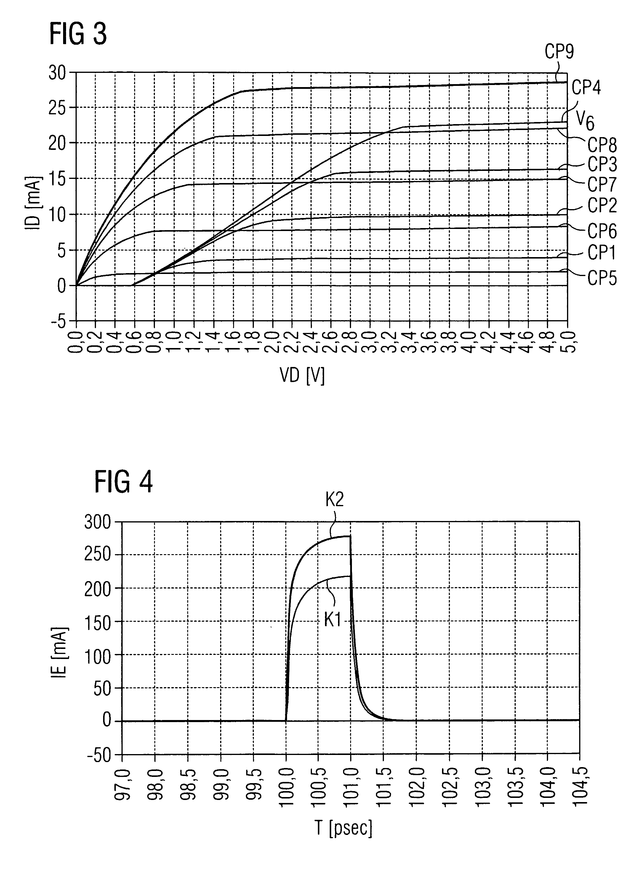
[0014] In the following description further aspects and embodiments of the present invention are summarized. In addition, reference is made to the accompanying drawings, which form a part hereof, and in which is shown by way of illustration, in which the invention may be practiced. The embodiments of the drawings present a summary in order to provide a better understanding of one or more aspects of the present invention. This summary is not an extensive overview of the invention and neither intended to limit the features or key-elements of the invention to a specific embodiment. Rather, the different elements, aspects and features disclosed in the embodiments can be combined in different ways by a person skilled in the art to achieve one or more advantages of the present invention. It is to be understood that other embodiments may be utilized and structural or logical changes may be made without departing from the scope of the present invention. The elements of the drawing are not n...


PUM


Abstract

A buffer circuit includes a signal input, a first and a second voltage tap and an inverter circuit including an inverter input coupled to the signal input, an output node and a first and a second supply tap. Furthermore, a first element having a diode-type transfer response is provided, which is coupled by an anode terminal to the first supply tap. The buffer circuit correspondingly includes a second element, which is coupled by a cathode terminal to the second supply tap. Furthermore, a transistor pair is provided, wherein a control terminal of a first transistor of the transistor pair is coupled to the anode terminal of the first element and a control terminal of a second transistor of the transistor pair is coupled to the cathode terminal of the second element.

Description

[0001] This application claims priority to German Patent Application 10 2005 050 624.0, which was filed Oct. 21, 2005 and is incorporated herein by reference. TECHNICAL FIELD [0002] The invention relates to a buffer circuit and to a use thereof. BACKGROUND [0003] Buffer circuits, in particular buffer circuits using complementary circuit technology (CMOS), are used for a multiplicity of digital circuits and are also referred to as push-pull circuits or as inverters for simplification. FIG. 5 shows a known example of a buffer circuit constructed from complementary field effect transistors for signal inversion. The buffer circuit illustrated comprises two series-connected field effect transistors T1, T2 of different conductivity types, which are coupled between two supply terminals VA1, VA2. The circuit is fed with a supply voltage via the two supply terminals. [0004] A connection node of the two transistors T1, T2 forms the output tap A for the output signal. In the present case, the ...

Claims


Application Information

Patent Timeline
IPC IPC(8): H03K19/094
CPCH03K19/0013H03K19/00384H03K19/01707
Inventor JOODAKI, MOJTABA
Owner QIMONDA
Why Eureka
Try Eureka