Laterally-integrated waveguide photodetector apparatus and related coupling methods

a waveguide and photodetector technology, applied in the field of fabrication of waveguide-based photodetector devices, can solve problems such as marginally and if, and achieve the effect of high data ra

Inactive Publication Date: 2007-05-10
MASSACHUSETTS INST OF TECH
View PDF18 Cites 178 Cited by
  • Summary
  • Abstract
  • Description
  • Claims
  • Application Information

AI Technical Summary

Benefits of technology

[0009] Heterointegration of lattice-mismatched materials is desirable for various electronic and optoelectronic applications. For example, as mentioned above, the possibility of the heterointegration of III-V, II-VI materials, and/or Ge with Si is an attractive path for fabricating integrated devices transmitting optical signals and converting them to electrical signals...

Problems solved by technology

Selective epitaxy is particularly suitable for such integration because it allows adding the non-Si semiconductor materia...

Method used


Image

  • Laterally-integrated waveguide photodetector apparatus and related coupling methods
  • Laterally-integrated waveguide photodetector apparatus and related coupling methods
  • Laterally-integrated waveguide photodetector apparatus and related coupling methods

Examples


Embodiment Construction

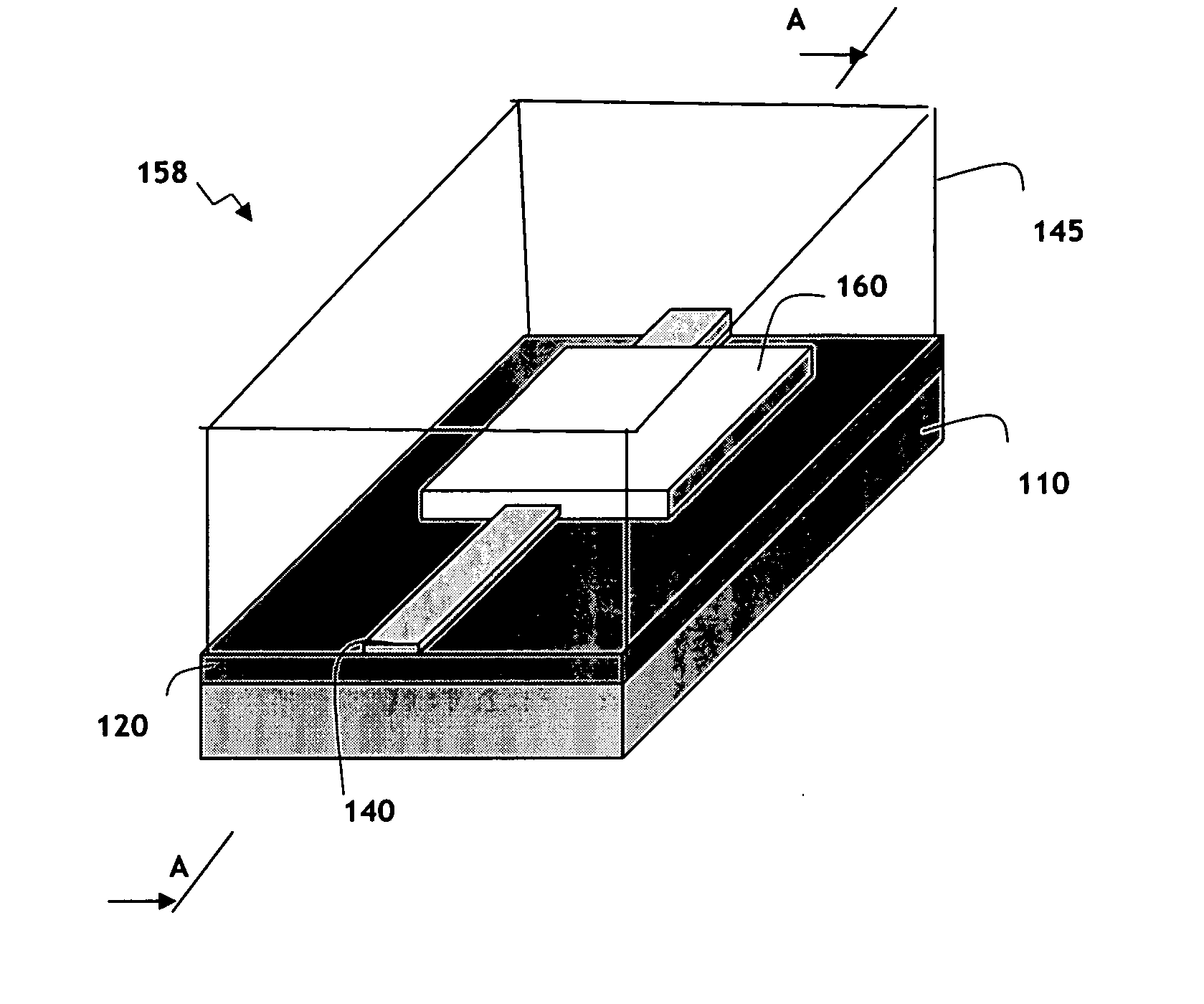
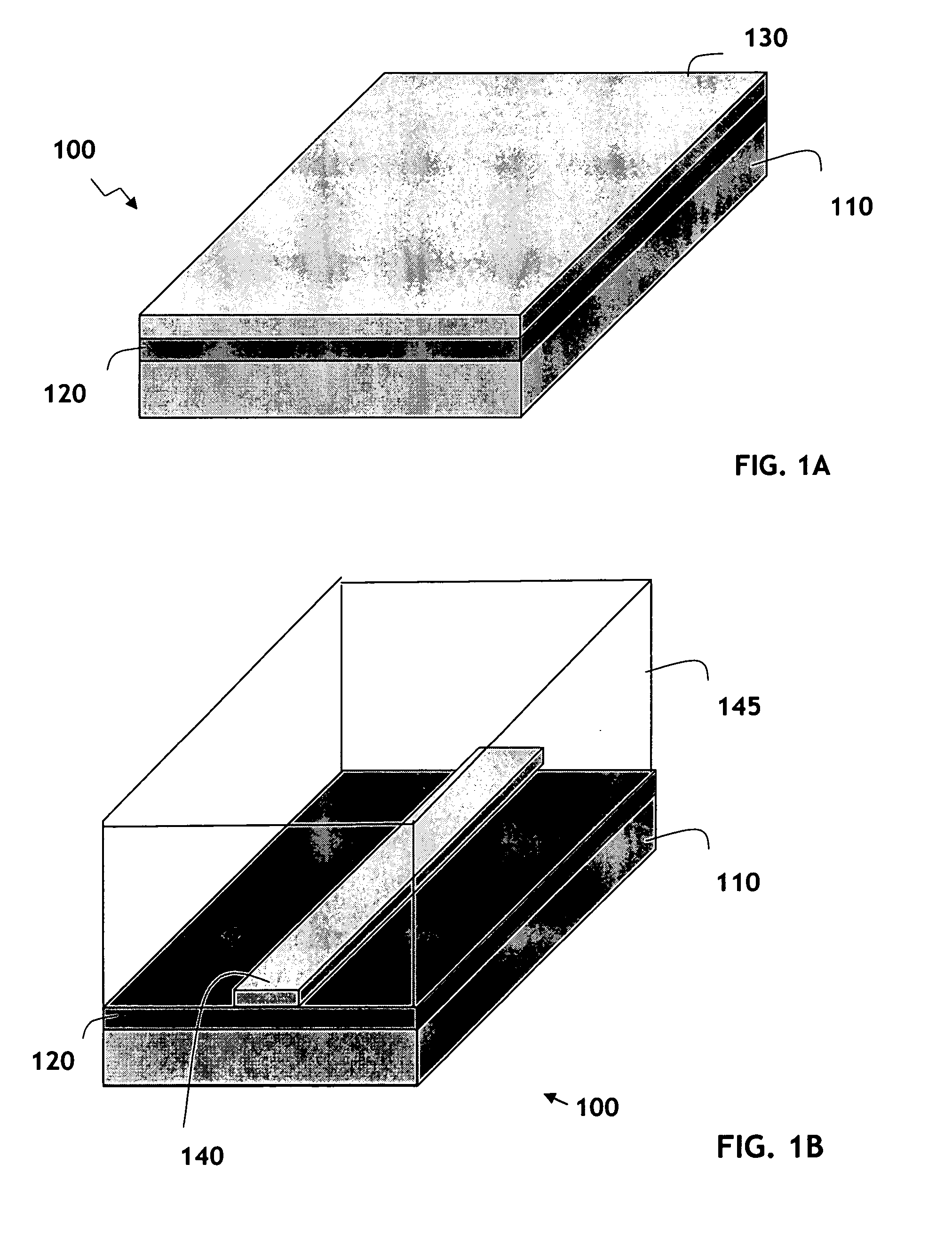
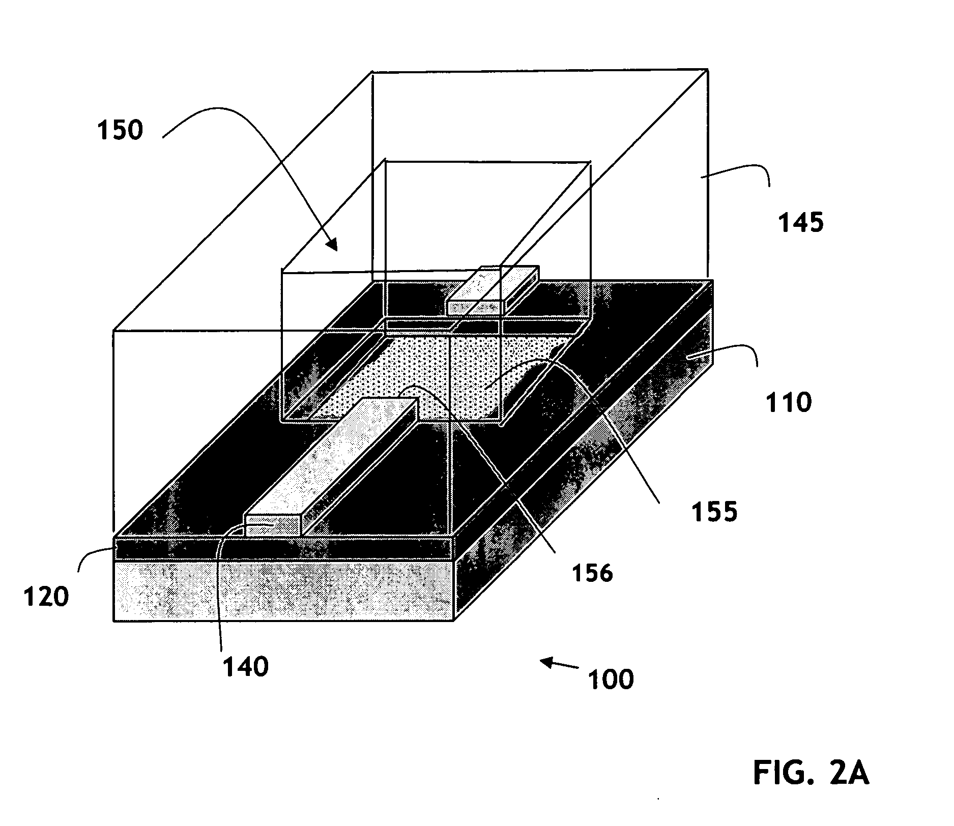
[0027] In accordance with its various embodiments, the invention disclosed herein contemplates fabrication of integrated waveguide-based photodetector apparatus with improved detection capabilities and integration density utilizing methods that are generally compatible with CMOS processing techniques. Also contemplated are optoetectronic circuits including at least one integrated photodetector apparatus, a light source for directing a lightwave thereto, and one or more electronic devices for receiving and processing an electrical signal generated in the photodetector apparatus.

[0028] As discussed in more detail below, efficient coupling between components in the integrated apparatus of the invention is facilitated by epitaxially growing a photodetector in lateral alignment with an optical waveguide. Selective epitaxy is suitable for fabricating optoelectronic devices according to many embodiments of the invention because it is only marginally, if at all, disruptive to a conventiona...


PUM


Abstract

High-speed optoelectronic devices having a waveguide densely integrated with and efficiently coupled to a photodetector are fabricated utilizing methods generally compatible with CMOS processing techniques. In various implementations, the waveguide consists essentially of single-crystal silicon and the photodetector contains, or consists essentially of, epitaxially grown germanium or a silicon-germanium alloy having a germanium concentration exceeding about 90%.

Description

FIELD OF THE INVENTION [0001] This invention relates generally to optoelectronic devices and, specifically, to methods and materials for fabrication of waveguide-based photodetector devices. BACKGROUND OF THE INVENTION [0002] Various optoelectronic applications, such as optical telecommunications and intra-chip interconnects, involve transmitting optical signals and converting them to electrical signals at high data rates. Systems for performing such transmission and conversion usually require photodetector devices compatible with the speed and bandwidth of the optical signal. Typically, these devices are PIN detectors—i.e. semiconductor devices including an intrinsic region sandwiched between a p-type region and an n-type region—that have frequency response in the GHz range and utilize optical waveguides as a conduit for directing light to the intrinsic region of the photodetector. [0003] Generally, an optical waveguide is a planar, rectangular, or cylindrical structure having a hi...

Claims


Application Information

Patent Timeline
IPC IPC(8): G02B6/10G02B6/26G02B6/42
CPCG02B6/12004G02B6/4204G02B2006/12178H01L31/105
Inventor AHN, DONGHWANLIU, JIFENGMICHEL, JURGENKIMERLING, LIONEL C.
Owner MASSACHUSETTS INST OF TECH
Why Eureka
Try Eureka