Method of controlling nanowire growth and device with controlled-growth nanowire

a nanowire and nanowire technology, applied in the direction of crystal growth process, coating, chemistry apparatus and processes, etc., can solve the problems that the vertical growth of nanowires from a (100)-oriented semiconductor has not been shown to be reproducible or practical

Inactive Publication Date: 2007-05-10
HEWLETT PACKARD DEV CO LP
View PDF7 Cites 60 Cited by
  • Summary
  • Abstract
  • Description
  • Claims
  • Application Information

AI Technical Summary

Problems solved by technology

Vertical growth of nanowires from a (100) planar surface of the [100]-oriented semiconductor has not been shown to be reproducible or practical.
Moreover, vertic...

Method used


Image

  • Method of controlling nanowire growth and device with controlled-growth nanowire
  • Method of controlling nanowire growth and device with controlled-growth nanowire
  • Method of controlling nanowire growth and device with controlled-growth nanowire

Examples


Embodiment Construction

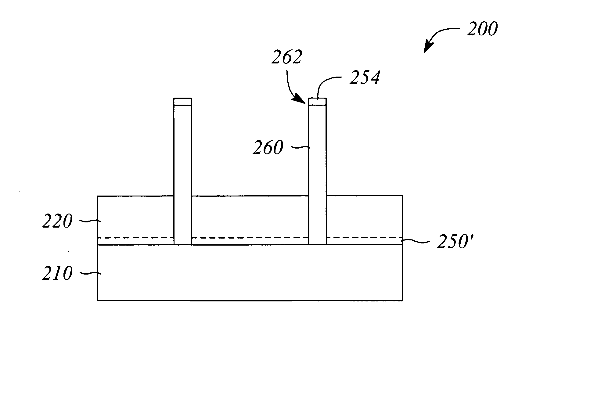
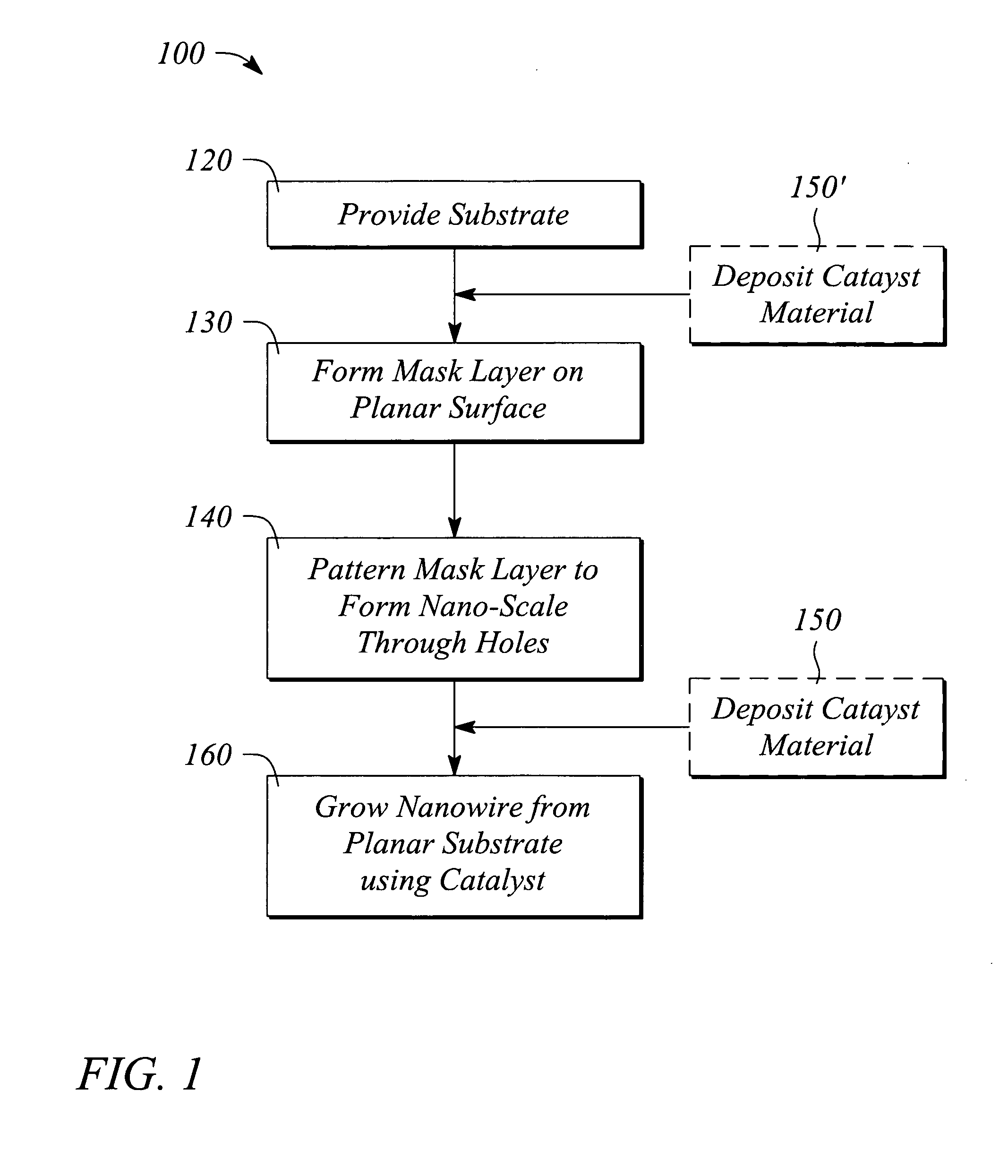
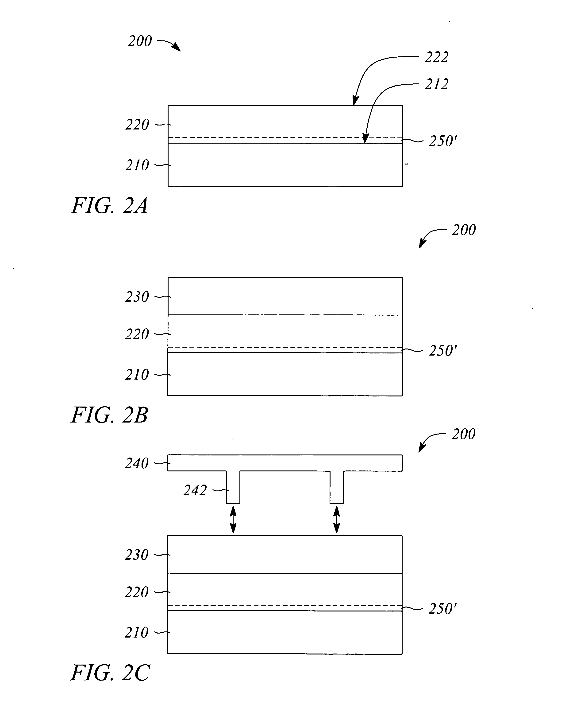
[0019] The embodiments of the present invention facilitate control over one or both of direction and location of nanowires grown using catalyzed growth from planar surfaces of a variety of substrates having one or more of crystalline regions having any crystal orientation, polycrystalline regions and non-crystalline regions. Some embodiments may facilitate control over uniformity of such nanowires including controlling one or both of uniform shape and uniform size. Semiconductor nanowires have been successfully grown from and perpendicular to (111) planar semiconductor surfaces using metal-catalyzed growth to provide an in situ interconnection in semiconductor structures between spaced apart layers (i.e., between circuit elements or components formed in or on a semiconductor structure). See, for example, co-pending U.S. patent application Ser. No. 10 / 982,051, filed Nov. 5, 2004, incorporated by reference herein.

[0020] While very promising, in situ vertical growth has been essential...


PUM

PropertyMeasurementUnit
Areaaaaaaaaaaa
Crystal orientationaaaaaaaaaa

Abstract

Nanowire growth in situ on a planar surface, which is one of a crystalline surface having any crystal orientation, a polycrystalline surface and a non-crystalline surface, is controlled by guiding catalyzed growth of the nanowire from the planar surface in a nano-throughhole of a patterned layer formed on the planar surface, such that the nanowire grows in situ perpendicular to the planar surface. An electronic device includes first and second regions of electronic circuitry vertically spaced by the patterned layer. The nano-throughhole of the patterned layer extends perpendicularly between the regions. The first region has the planar surface. The device further includes a nanowire extending perpendicular from a catalyst location on the planar surface of the first region in the nano-throughhole. The nanowire forms a component of a nano-scale circuit that connects the regions.

Description

STATEMENT REGARDING FEDERALLY SPONSORED RESEARCH OR DEVELOPMENT [0001] The U.S. Government has a paid-up license in this invention and the right in limited circumstances to require the patent owner to license others on reasonable terms as provided for by the terms of Contract No. MDA972-01-3-0005 awarded by the Defense Advanced Research Projects Agency.CROSS-REFERENCE TO RELATED APPLICATIONS [0002] N / A BACKGROUND [0003] 1. Technical Field [0004] The invention relates to nano-scale semiconductor devices and fabrication methods therefor using nanowires. In particular, the invention relates to control of fabrication of nanowires and their use in semiconductor devices. [0005] 2. Description of Related Art [0006] A consistent trend in semiconductor technology since its inception is toward smaller and smaller device dimensions and higher and higher device densities. As a result, an area of semiconductor technology that recently has seen explosive growth and generated considerable interest...

Claims


Application Information

Patent Timeline
IPC IPC(8): H01L21/20H01L21/44C30B11/00
CPCH01L21/28525H01L21/76879H01L23/53276H01L2221/1094H01L2924/0002H01L2924/00
Inventor WU, WEIKAMINS, THEODORE I.SHARMA, SHASHANKWILLIAMS, R. STANLEY
Owner HEWLETT PACKARD DEV CO LP
Why Eureka
Try Eureka