
LED package

Inactive Publication Date: 2007-05-17
SAMSUNG ELECTRO MECHANICS CO LTD
View PDF1 Cites 17 Cited by
  • Summary
  • Abstract
  • Description
  • Claims
  • Application Information

AI Technical Summary

Benefits of technology

[0017] The present invention has been made to solve the foregoing problems of the prior art and it is therefore an object according to certain embodiments of the present invention is to provide a light emitting diode package which ensures a sufficient view angle of light generated from a light emitting chip to improve light extraction efficiency and a simplified assembly process to achieve mass production and save manufacturing costs.

Problems solved by technology

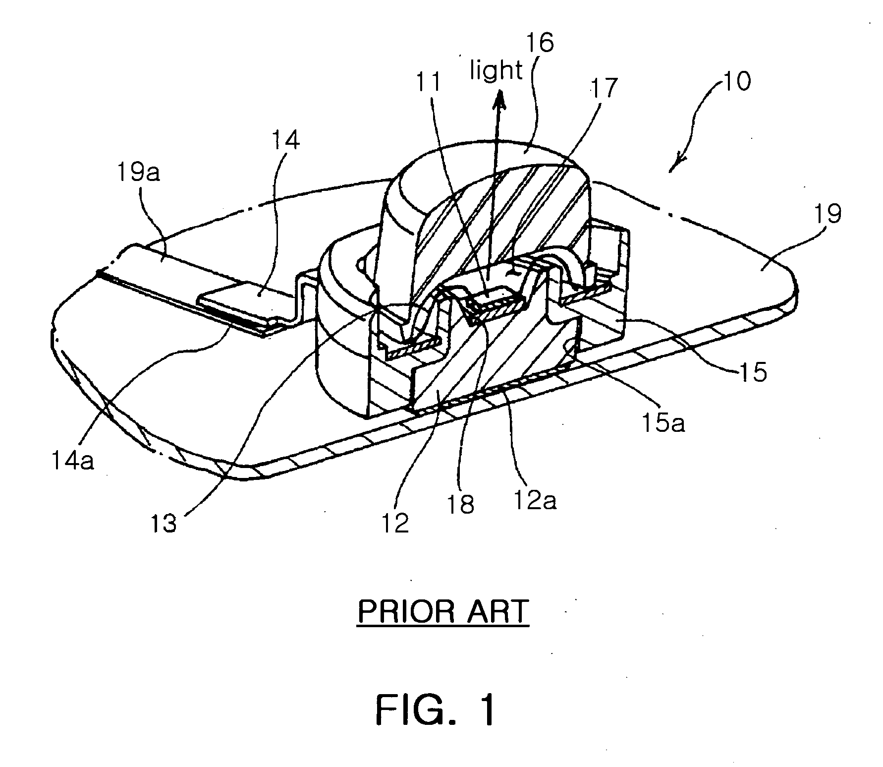
However, it is a complicated process to dispose the separately manufactured lens 16 on the molding 15 and fill the filler 17 between the lens 16 and molding 15.
This accordingly undermines work productivity.
In addition, when the lens 16 is mounted, the filler 17 is leaked outside or bubbles are trapped inside the filler 17, thereby lowering optical efficiency.
Moreover, the lens 16, made of polymer, experiences degradation due to high energy light generated from the light emitting chip 11, thereby shortening useful life of the product.
On the other hand, the lens 16, made of silicone, is expensive in manufacturing costs.

Method used


Image

  • LED package
  • LED package
  • LED package

Examples


Embodiment Construction

[0030] Preferred embodiments of the present invention will now be described in detail with reference to the accompanying drawings.

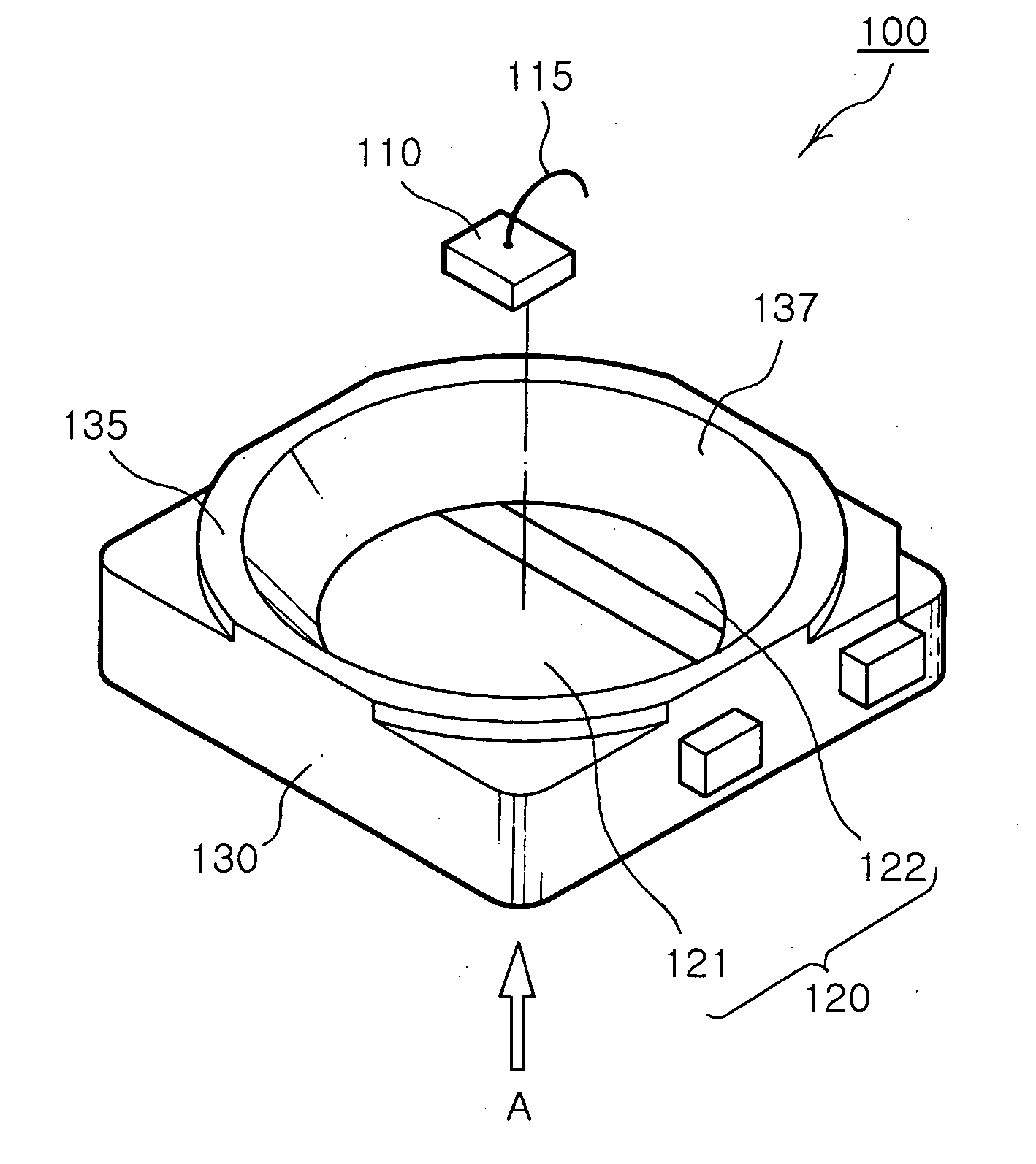
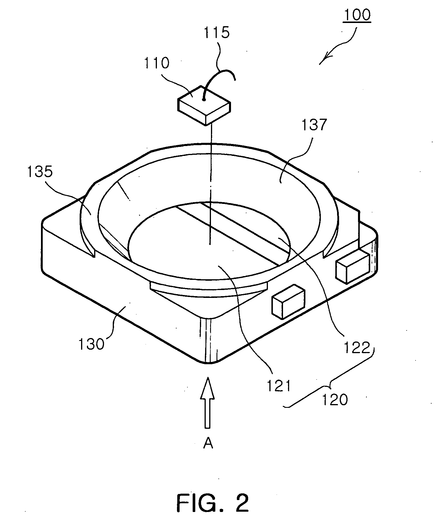
[0031]FIG. 2 is a perspective view illustrating an LED package according to the invention. FIG. 3 is a side elevation view seen from an arrow A direction of FIG. 2. FIG. 4 is a plan view illustrating an LED package according to the invention.

[0032] As shown in FIGS. 2 to 4, the LED package 100 of the invention does not require a complicated process for assembling a separately manufactured lens. But in a simpler manufacturing process, the LED package 100 of the invention has a resin filled to cover a light emission source in an upward dome shape. This serve to widen a view angle of the LED package 100. The LED package 100 of the invention includes a light emitting chip 110, a frame 120, a molding and a lens 140.

[0033] The light emitting chip 110 emits light when current is applied and generates heat when emitting light.

[0034] Such a light emitting chip...


PUM


Abstract

An LED package is provided. A light emitting chip generates light when current is applied. A frame is electrically connected to the light emitting chip via a wire, and has the light emitting chip mounted thereon. A molding fixes the frame thereto, and has a cavity surrounding the light emitting chip and an embossed protrusion formed on a top surface thereof. A lens is domed upward from the embossed protrusion along an outer periphery of the embossed protrusion. The lens is made of a light transmissible resin filled in the cavity. The invention ensures a sufficient view angle of light generated from the LED chip, thereby increasing light extraction efficiency. This consequently simplifies an assembly process, allowing mass production and reducing manufacturing costs.

Description

CLAIM OF PRIORITY [0001] This application claims the benefit of Korean Patent Application No. 2005-108909 filed on Nov. 15, 2005 in the Korean Intellectual Property Office, the disclosure of which is incorporated herein by reference. BACKGROUND OF THE INVENTION [0002] 1. Field of the Invention [0003] The present invention relates to a light emitting diode package, more particularly, which ensures a sufficient view angle of light generated from a light emitting chip to improve light extraction efficiency and simplify an assembly process, thereby achieving mass production and reducing manufacturing costs. [0004] 2. Description of the Related Art [0005] In general, a light emitting diode (LED) package is a semiconductor device which emits light when current is applied, by converting an electrical energy into a light energy via a PN junction diode made of a GaAs or GaN optical semiconductor. [0006] Such an LED emits various lights ranging from red light in the wavelength of 630 nm to 70...

Claims


Application Information

Patent Timeline
IPC IPC(8): H01L33/00H01L29/22H01L33/54H01L33/56H01L33/60H01L33/62
CPCH01L33/486H01L33/54H01L33/56H01L33/60H01L2933/0091H01L2224/48091H01L2224/48247H01L2924/00014
Inventor LEE, SEON GOOCHOI, MYOUNG SOOSONG, CHANG HOPARK, YOUNG SAM
Owner SAMSUNG ELECTRO MECHANICS CO LTD
Learn More