Photoelectric converter and imaging system including the same

a technology of photoelectric converter and imaging system, applied in the field of photoelectric converter, can solve the problems of complex fabrication process, complicated patterning process, and complicated process, and achieve the effect of simplifying the process of forming antireflection film and etch stop film

Inactive Publication Date: 2007-05-17
CANON KK
View PDF19 Cites 15 Cited by
  • Summary
  • Abstract
  • Description
  • Claims
  • Application Information

AI Technical Summary

Benefits of technology

[0010] The present invention is directed to a photoelectric converter in which the process of forming an antireflection film and an etch stop film can be simplified.

Problems solved by technology

However, with the reduction in size of photoelectric converters, the percentage of the area taken up by the element isolation regions in the total area is increasing excessively, thus causing problems.
However, to fabricate the structure in which the etch stop film is disposed on at least a part of the buried insolating film in the element isolation region, a complicated process is required.
Specifically, since the etch stop film is not provided at the position where a contact is formed, the patterning process becomes complicated.
In such a case, since the antireflection film and the etch stop film are separately formed, the fabrication process becomes further complicated.

Method used


Image

  • Photoelectric converter and imaging system including the same
  • Photoelectric converter and imaging system including the same
  • Photoelectric converter and imaging system including the same

Examples


first embodiment

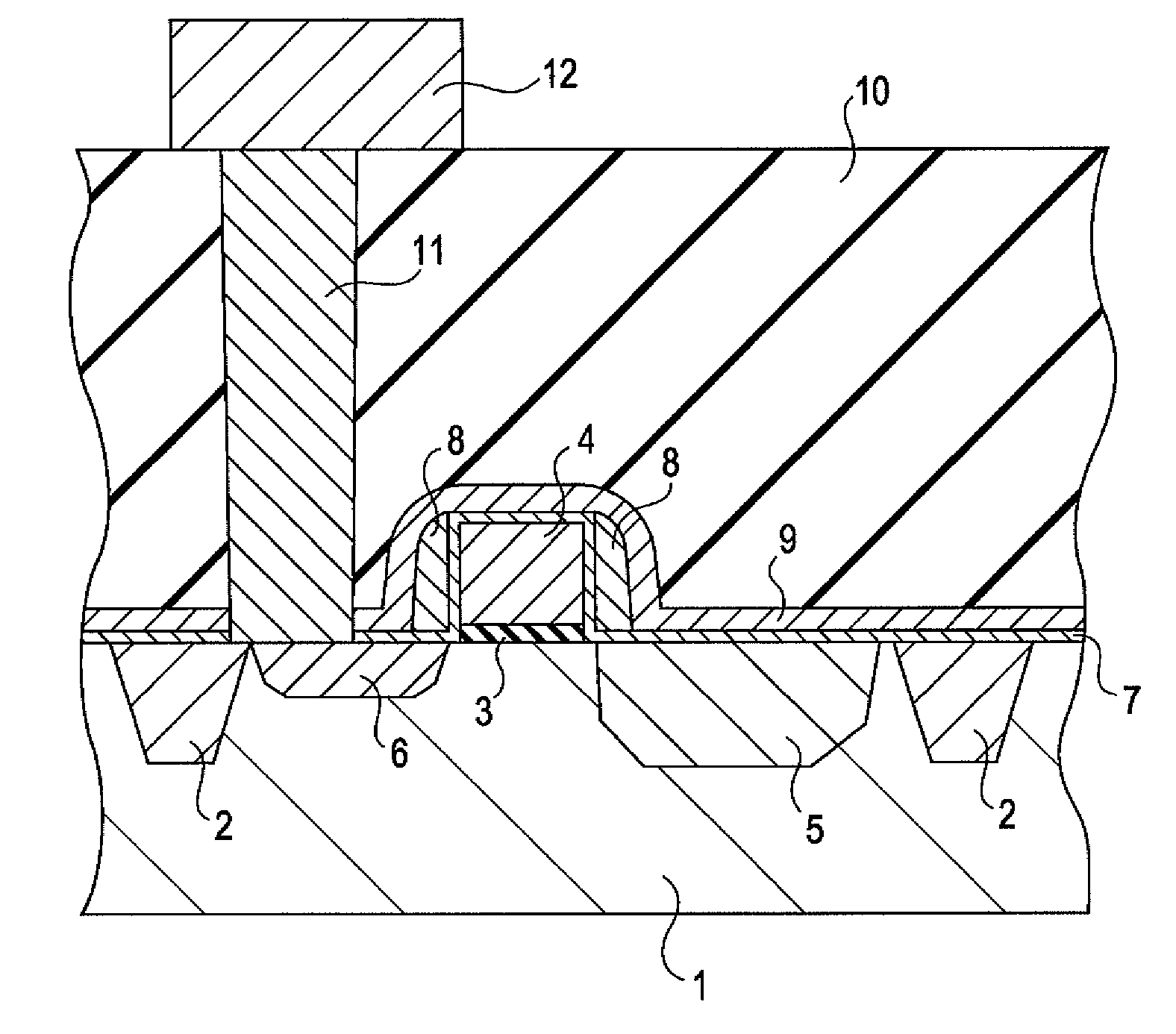
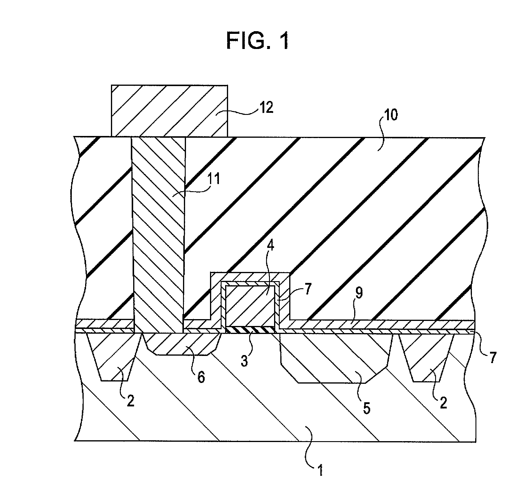
[0029]FIG. 1 is a cross-sectional view showing a substantial part of a photoelectric converter according to a first embodiment. This cross-sectional view corresponds to that taken along the line A-B in FIG. 4B.

[0030]FIG. 1 shows a substantial part of a photoelectric converter in which a photodiode and MOS transistor are disposed. In the actual photoelectric converter, wiring layers connected to a gate electrode 4 and the like are provided, which are not shown in FIG. 1.

[0031] In the photoelectric converter according to this embodiment, on the surface of a silicon substrate 1, which is, for example, a first-conductivity-type semiconductor substrate, a semiconductor region 5 of a conductivity type opposite the first conductivity type (i.e., second conductivity type) is disposed. The second-conductivity-type semiconductor region 5 has the same conductivity type as that of signal electric charges and accumulates signal electric charges. The semiconductor region 5 constitutes a photoel...

second embodiment

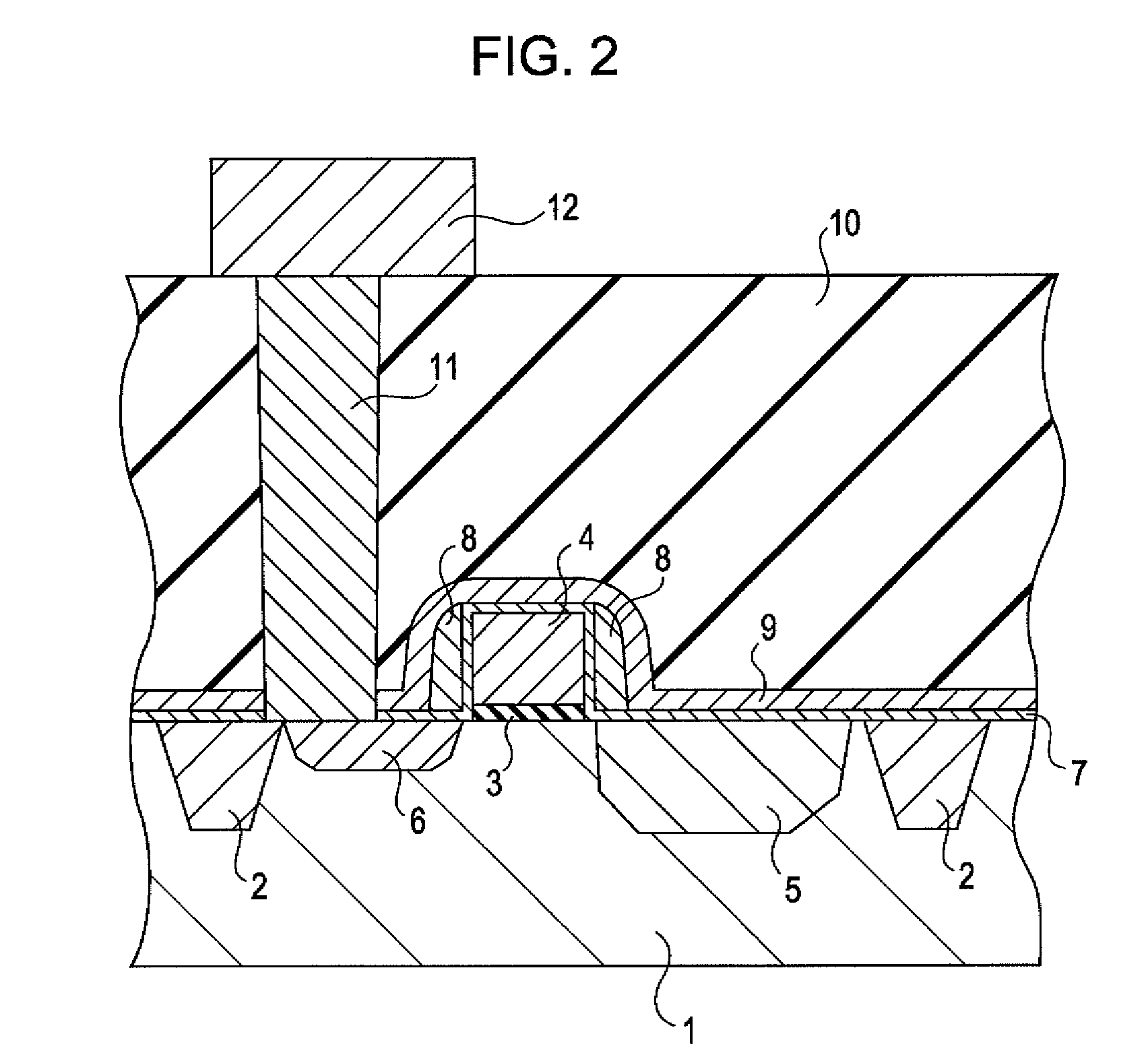
[0038] A second embodiment will be described with reference to FIG. 2. In FIG. 2, the parts having the same functions as those in the first embodiment shown in FIG. 1 are represented by the same reference numerals, and the description thereof will be omitted. This embodiment differs from the first embodiment in that a sidewall 8 is disposed on the side face of the gate electrode 4 with the silicon oxide film 7 therebetween. For example, a silicon nitride film is used as an insulating film for the sidewall 8.

[0039] That is, two types of insulating films (silicon oxide film 7 and silicon nitride films 8 and 9) are provided as a sidewall on the gate electrode 4. The difference in stress between the silicon nitride film 8 and the silicon substrate 1 or the gate electrode 4 is reduced by the silicon oxide film 7.

[0040] As in the first embodiment, the silicon nitride film 9 is arranged above at least the light-receiving surface of the photoelectric converting element and is arranged so ...

third embodiment

[0041] After the silicon nitride film 9, such as that shown in the first embodiment, which functions as the antireflection film and the etch stop film, is formed so as to cover the entire surface including a peripheral circuit portion, the silicon nitride film 9 is etched back only in the peripheral circuit portion. Thus, using the sidewalls composed of the resulting silicon nitride film, it is possible to allow the transistors in the peripheral circuit portion to have an LDD structure.

[0042] The peripheral circuit portion corresponds to scanning circuits for driving the MOS transistors and circuits for reading signals from the pixels. Examples include the clamp circuit, the column amplifier portion, the signal holding portion including the capacitors 112a and 112b, and the scanning circuits 119 and 123, which are shown in FIG. 4A.

[0043] The silicon nitride film 9 formed on the pixel area 124 is not subjected to etching and is protected with a mask or the like. By using such a str...


PUM


Abstract

A photoelectric converter includes a substrate, photoelectric converting elements formed in the substrate and each having a light-receiving surface, an antireflection film arranged above at least a part of the light-receiving surface of each photoelectric converting element, an element isolation region including an insulator, a plurality of transistors including read transistors configured to read electric charges of the photoelectric converting elements, an interlayer insulating film arranged above the photoelectric conversion elements and the read transistors, and contacts electrically connected to active regions of the transistors. The antireflection film is arranged above the element isolation region and the active region connected to each contact. The antireflection film serves as an etch stop film when the interlayer insulating film is etched.

Description

BACKGROUND OF THE INVENTION [0001] 1. Field of the Invention [0002] The present invention relates to a photoelectric converter including photoelectric converting elements and semiconductor elements that are different from the photoelectric converting elements. More particularly, the invention relates to a photoelectric converter in which reflection at the light-receiving surfaces of the photoelectric converting elements is reduced. [0003] 2. Description of the Related Art [0004] In a photoelectric converter, photoelectric converting elements, circuits for amplifying signals from the photoelectric converting elements, and the like are one-dimensionally or two-dimensionally arrayed on a substrate. As photosensors which convert optical signals into electrical signals, photoelectric converters are, for example, used as control photosensors in various photoelectric converting apparatuses and mounted on digital cameras, video cameras, copiers, facsimile machines, and the like. [0005] In t...

Claims


Application Information

Patent Timeline
Patent Type & Authority Applications(United States)
IPC IPC(8): H01L31/06
CPCH01L27/14603H01L27/1462H01L27/1463H01L27/14636H01L27/14687
Inventor FURUICHI, AIKO
Owner CANON KK
Why Eureka
Try Eureka