

Second Schottky contact metal layer to improve GaN Schottky diode performance
- Summary
- Abstract
- Description
- Claims
- Application Information
AI Technical Summary
Benefits of technology
Problems solved by technology
Method used
Image

Examples
Embodiment Construction
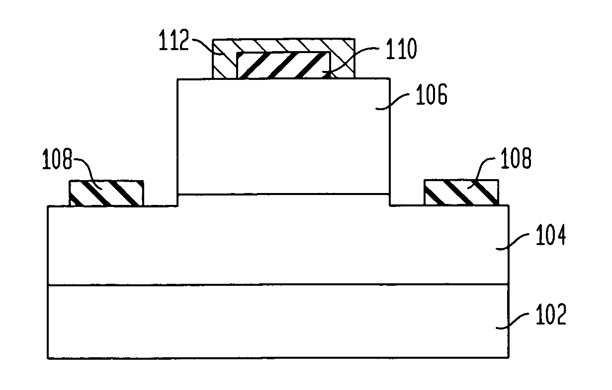
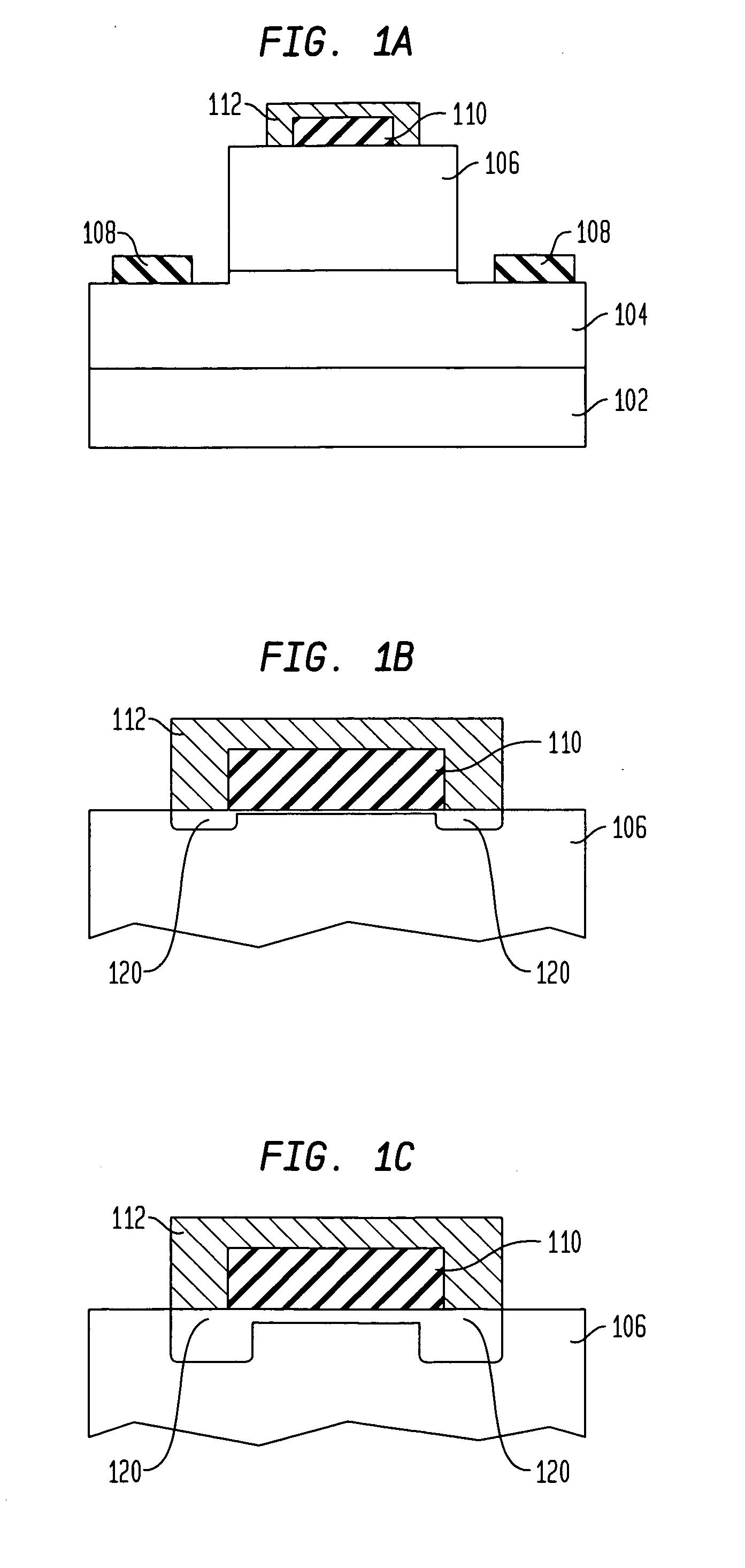
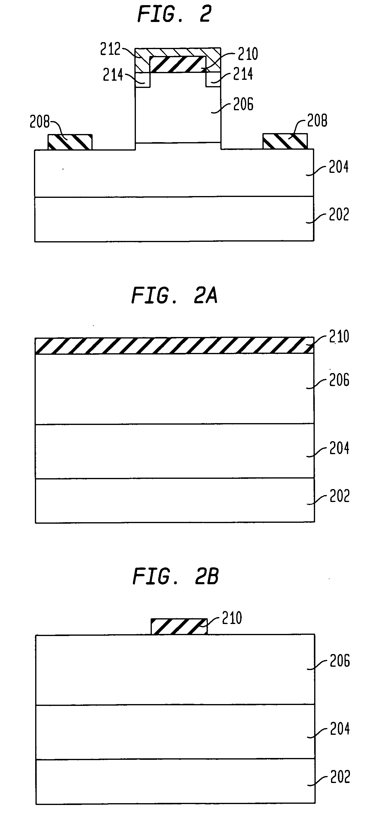
[0020] The present invention provides a Schottky diode having two deposited Schottky contact metals to improve device performance when the device is reverse biased while maintaining substantially the same forward voltage drop values when the device is forward biased. The first Schottky contact metal has relatively small metal work function whereas the second Schottky contact metal has relatively high metal work function. When the device is forward biased, most of the Schottky contact has a small barrier height because of the first Schottky contact metal's reduced contact resistance which , as a result, improves current flow. When the device is reverse biased, the effect of the high work function second Schottky contact metal dominates and results in a high reverse blocking voltage VR.
[0021] As used in the present disclosure, the term “III-V semiconductor” refers to a compound semiconductor material according to the stoichiometric formula AlaInbGacNdAsePf where (a+b+c) is about 1 an...
PUM
 Abstract
Description
Claims
Application Information