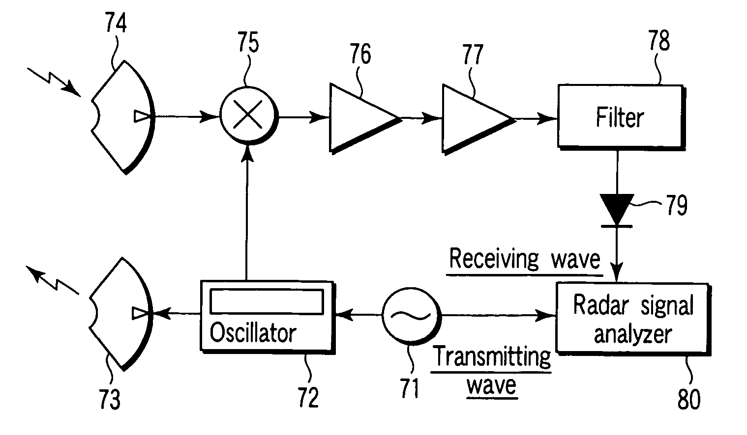
This helps you quickly interpret patents by identifying the three key elements:
Problems solved by technology
Method used
Benefits of technology
[0011] A high-frequency oscillator according to an aspect of the present invention comprises: a high-frequency oscillation element comprising a magnetization pinned layer whose magnetization direction is pinned substantially in one direction; an oscillation layer formed of a magnetic material which generates a high-frequency oscillation phenomenon when a current is supplied; an intermediate laye
Problems solved by technology
In the case where millimeter wave band or microwave band is used for communication or radar applications, it is unlikely to be subject to influences of weather or powder dust.
However, such a millimeter-wave oscillator must have a complicated structure (see, for example, JP-A-2005-19570), which has been a problem.
As a consequence, it is difficult to realize a compact high-frequency filter, and it is also difficult to apply a superconductive element to consumer products from the viewpoint of cost.
Howev
Method used
Image
Click on the blue label to locate the original text in one second.
Reading with bidirectional positioning of images and text.
Examples
examples
[0054] Examples of the present invention will be described in more detail with reference to the accompanying drawings hereinafter. In the following examples, symbol “%” representing a composition of an alloy means atomic %
embodiment 1
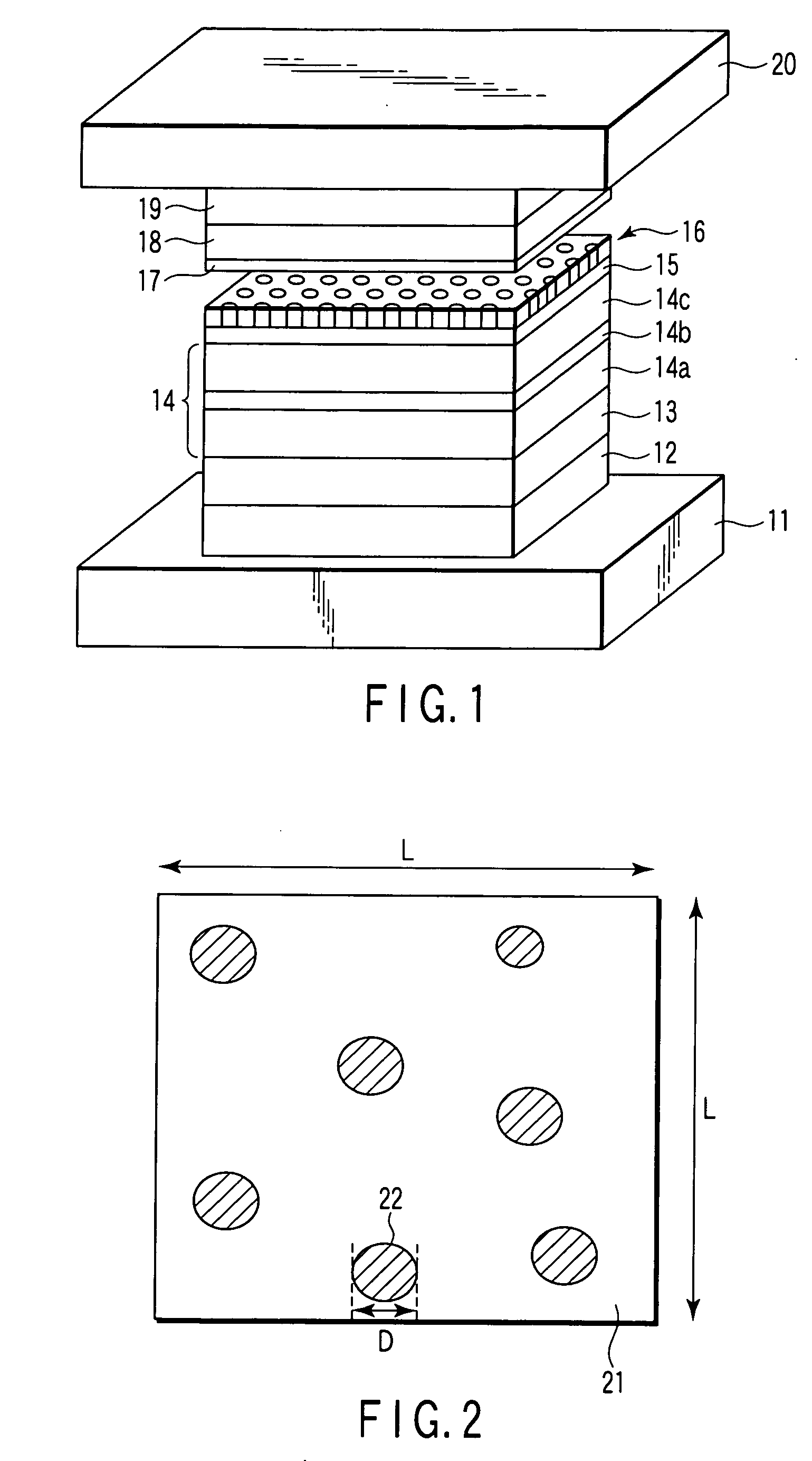
[0055] In Example 1, a specific example of a high-frequency oscillator (CCP-CPP element) having the structure shown in FIG. 1 will be described. The high-frequency oscillator of the example is manufactured by stacking the following films sequentially on a substrate (not shown).
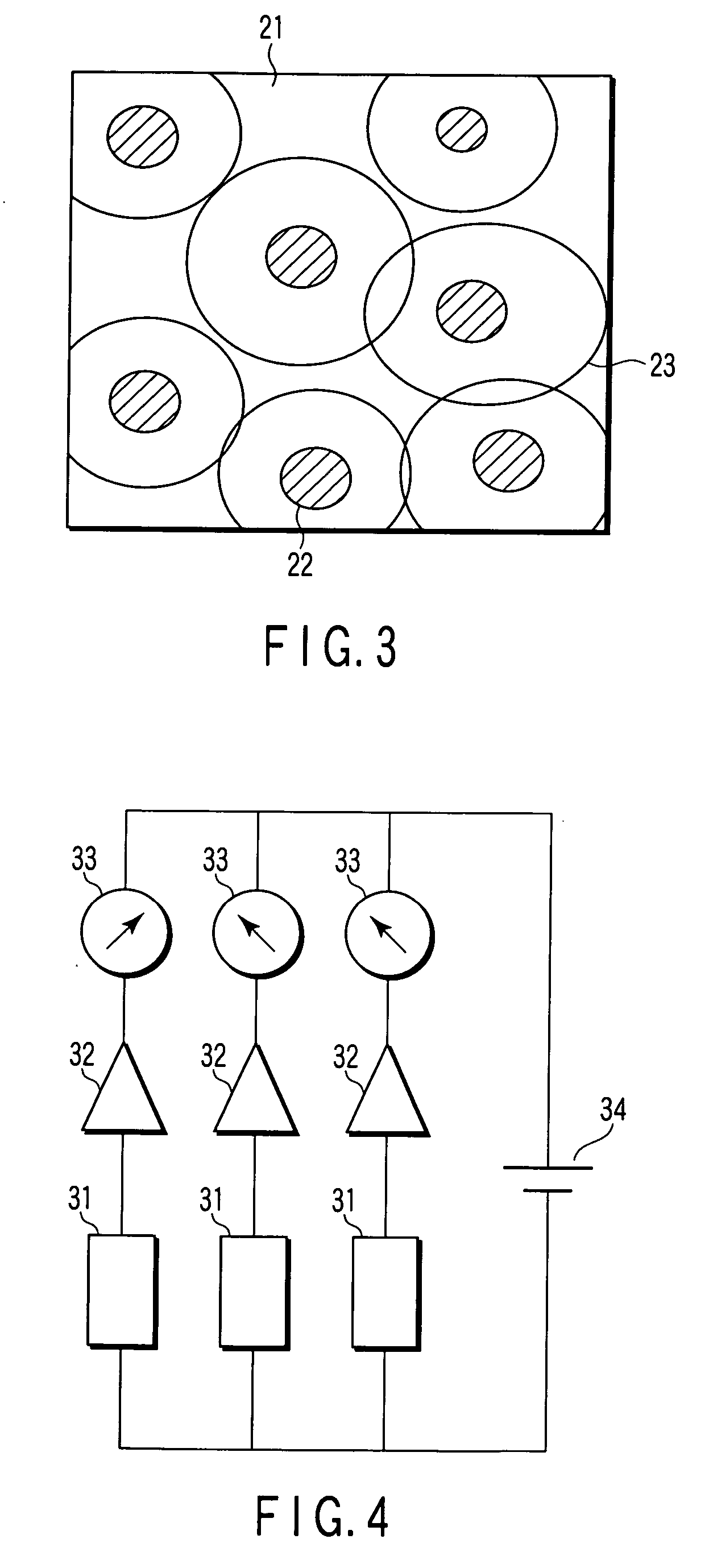
[0056] Spacer layer 16: Al2O3 insulation layer 21 and Cu current paths 22 (which is formed by a method of depositing a film of Al90Cu10 [1 nm], performing a pre-ion treatment before oxidization to apply ion beam of rare gas [PIT] and ion beam-assisted oxidization [IAO])
[0057] It should be noted that the spacer layer 16, the upper and lower metal layers 15 an...
embodiment 2
[0084]FIG. 8 shows a perspective view of a CCP-CPP oscillator according to a modified example of the present invention. The CCP-CPP oscillator has a structure in which stacked on a substrate (not shown) are a lower electrode 11, an underlayer 12, a first pinning layer 131, a first magnetization pinned layer (synthetic pinned layer) 141, a first intermediate layer 161, an oscillation layer 18, a second intermediate layer 162, a second magnetization pinned layer (synthetic pinned layer) 142, a second pinning layer 132, a cap layer 19, and an upper electrode 20.
[0085] In this CCP-CPP oscillator, the intermediate layers 161, 162 including nanoscopic current paths are provided on and under an oscillation layer 18 where spin waves are excited, and an oscillation output can be increased since the current confinement effect is high.
PUM
Abstract
A high-frequency oscillator includes a high-frequency oscillation element having a magnetization pinned layer whose magnetization direction is pinned substantially in one direction, an oscillation layer formed of a magnetic material which generates a high-frequency oscillation phenomenon when a current is supplied, an intermediate layer provided between the magnetization pinned layer and the oscillation layer, the intermediate layer having an insulation layer and current paths which pass through the insulation layer in a thickness direction, and a pair of electrodes which supply a current perpendicularly to a plane of a stacked film including the magnetization pinned layer, the intermediate layer and the oscillation layer.
Description
CROSS-REFERENCE TO RELATED APPLICATIONS [0001] This application is based upon and claims the benefit of priority from prior Japanese Patent Application No. 2005-314689, filed Oct. 28, 2005, the entire contents of which are incorporated herein by reference. BACKGROUND OF THE INVENTION [0002] 1. Field of the Invention [0003] The present invention relates to a high-frequency oscillator for use in a millimeter-wave-band or microwave-band radio communication apparatus, radar device and the like. [0004] 2. Description of the Related Art [0005] In the case where millimeter wave band or microwave band is used for communication or radar applications, it is unlikely to be subject to influences of weather or powder dust. Because it is of short wavelength, a transmitting / receiving antenna can be made compact. In addition, it enables to detect the relative speed to an object through the Doppler effect with high precision. For these reasons, in recent years, millimeter-wave radar has been started...
Claims
Application Information
Patent Timeline
Application Date:The date an application was filed.
Publication Date:The date a patent or application was officially published.
First Publication Date:The earliest publication date of a patent with the same application number.
Issue Date:Publication date of the patent grant document.
PCT Entry Date:The Entry date of PCT National Phase.
Estimated Expiry Date:The statutory expiry date of a patent right according to the Patent Law, and it is the longest term of protection that the patent right can achieve without the termination of the patent right due to other reasons(Term extension factor has been taken into account ).
Invalid Date:Actual expiry date is based on effective date or publication date of legal transaction data of invalid patent.