Liquid crystal display panel and fabricating method thereof

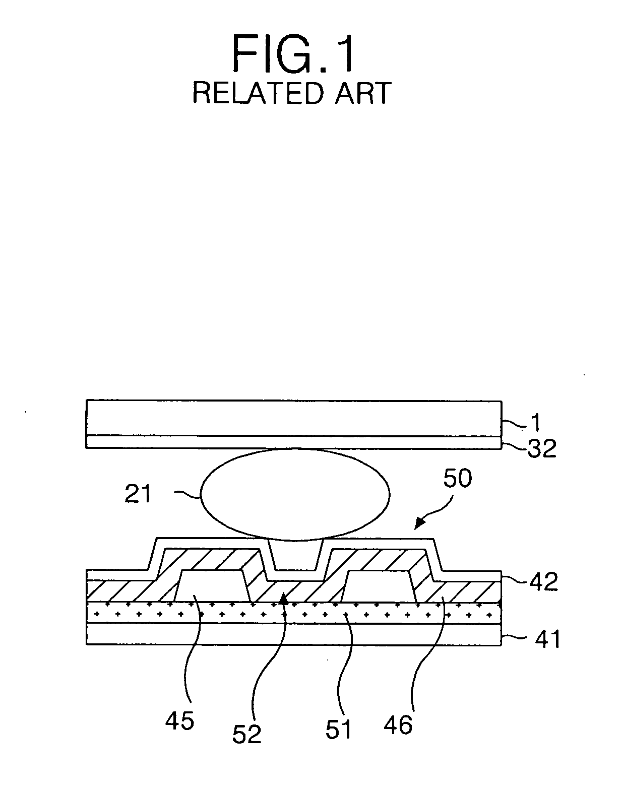
a technology fabrication method, which is applied in the field of liquid crystal display panel, can solve the problems of signal distortion, inferior picture quality, and easy separation of organic protective film and adhesive, and achieve the effect of minimizing the height of a space and minimizing the height of a silver do

Active Publication Date: 2007-05-17
LG DISPLAY CO LTD
View PDF2 Cites 21 Cited by
  • Summary
  • Abstract
  • Description
  • Claims
  • Application Information

AI Technical Summary

Benefits of technology

[0013] An advantage of the present invention is to provide a liquid crystal display panel and fabricating method thereof that minimize height of a silver dot necessary to completely electrically connect the silver dot and an electrode.
[0014] Additional features and advantages of the present invention will be set forth in the description which follows, and in part will be apparent from the description, or may be learned by practice of the invention. These and other advantages of the invention will be realized and attained by the structure particularly pointed out in the written description and claims hereof as well as the appended drawings.
[0015] To achieve these and other advantages, and in accordance with the purpose of the present invention, as embodied and broadly described, the liquid crystal display panel according to the present invention comprises: a common pad formed on a first substrate; a common electrode supplied with a common voltage through the common pad, on a second substrate opposite to the first substrate; a conductive dot formed between the common electrode and the common pad to be electrically connected to each other; and an organic protective film that minimizes a height of a space between the commmon pad and the common electrode.
[0016] The common pad may include a first pad electrode formed on the first substrate; the organic protective film substantially covering the first pad electrode; a first pad contact hole passing through the organic protective film to expose the first pad electrode; and a second pad electrode connected, through the first pad contact hole, to the first pad electrode, and that is formed on the organic protective film.
[0017] At least one first pad contact hole may be formed at an area overlapping with the conductive dot.
[0018] At least one first pad contact hole may be formed at a non-overlapping area of the conductive dot.

Problems solved by technology

However, a problem arises in that the organic protective film and an adhesive easily separate because of a weak contact force between the organic protective film and the adhesive.
Inferior picture quality results from the signal distortion.
Accordingly, poor picture quality results.
Further, it is difficult to vary the size of the silver dot given space limitations of the dot area.

Method used


Image

  • Liquid crystal display panel and fabricating method thereof
  • Liquid crystal display panel and fabricating method thereof
  • Liquid crystal display panel and fabricating method thereof

Examples


Embodiment Construction

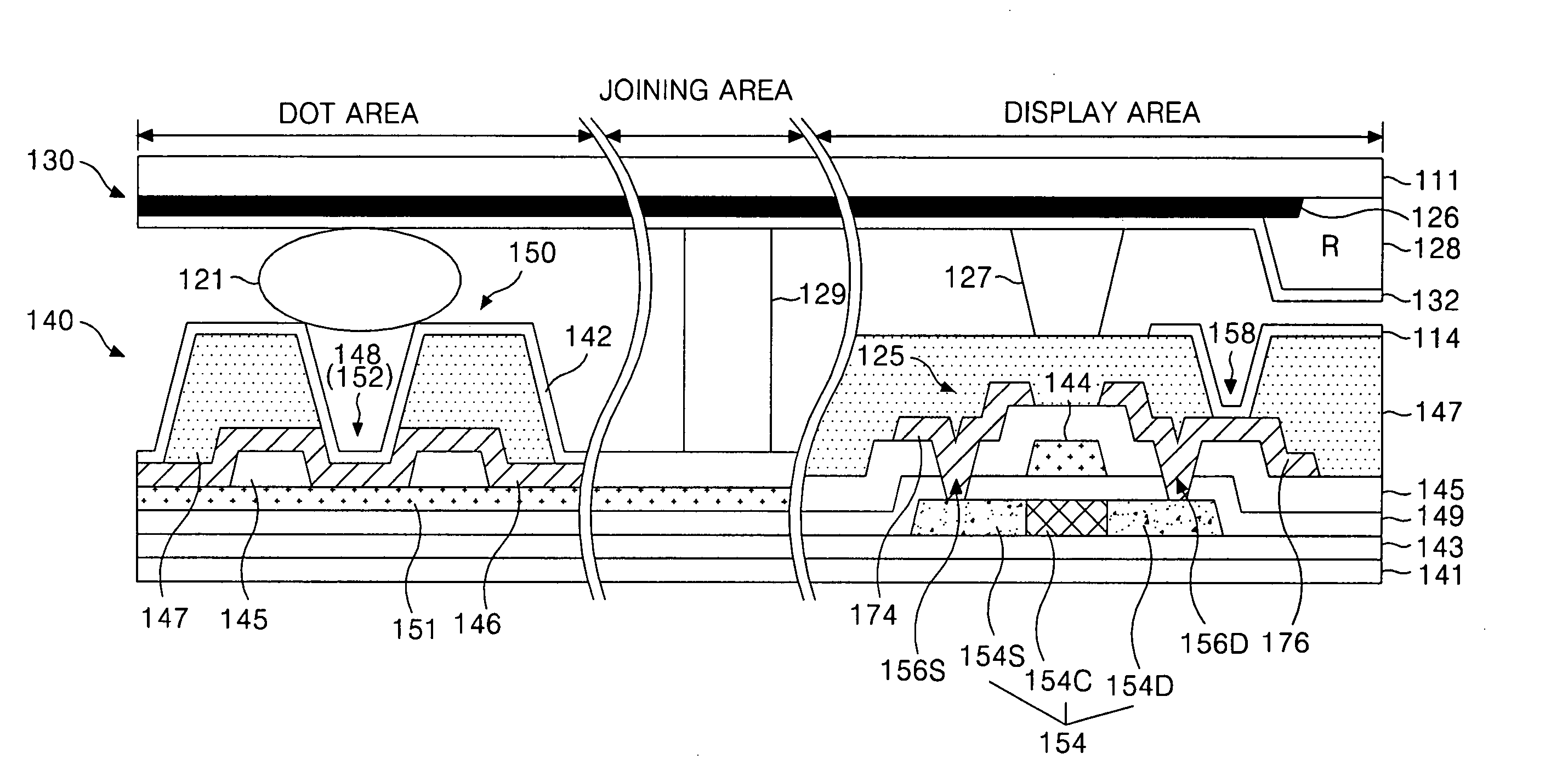
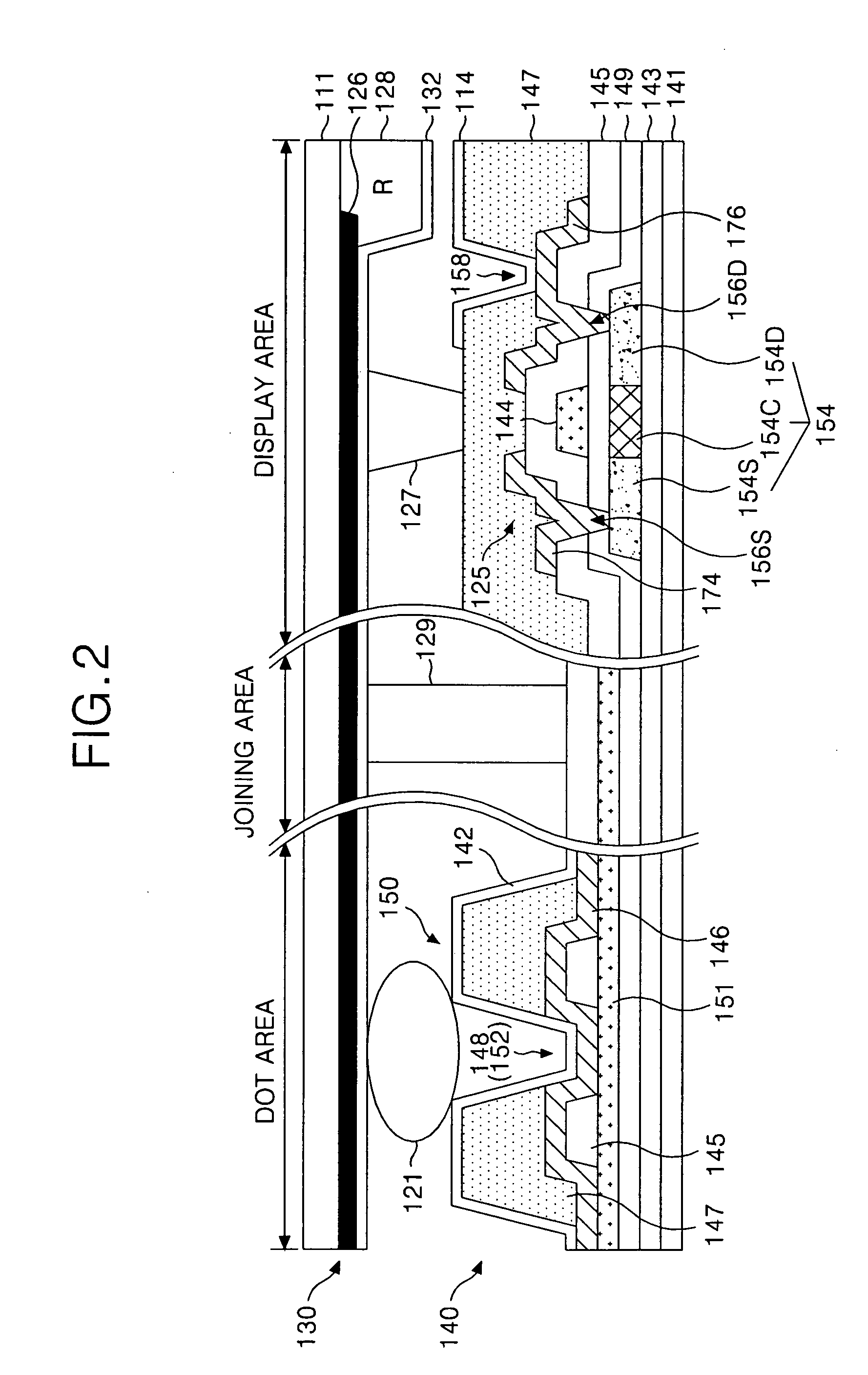
[0042] Hereinafter, the preferred embodiments of the present invention will be described in detail with reference to FIG. 2 through and including FIG. 5.

[0043]FIG. 2 is a sectional view showing a structure of a liquid crystal display panel according to an embodiment of the present invention.

[0044] Referring to FIG. 2, a liquid crystal display panel according to this embodiment of the present invention includes a color filter substrate 130, a thin film transistor substrate 140 joined with the color filter substrate 130 by an adhesive 129, and a silver dot 121 for supplying a common voltage to a common electrode 132 of the color filter substrate 130.

[0045] In the color filter substrate 130, a black matrix 126 for preventing light leakage, a color filter 128 for producing color and a common electrode 132 that forms a substantially vertical electric field along with a pixel electrode 114 are formed on an upper substrate 111. Also, in the color filter substrate 130, a column spacer 12...


PUM

PropertyMeasurementUnit
thicknessaaaaaaaaaa
thicknessaaaaaaaaaa
thicknessaaaaaaaaaa

Abstract

A liquid crystal display panel and a fabricating method thereof for minimizing a resistance of a silver dot caused by thickness of a silver dot and preventing distortion of a common voltage are disclosed. In the liquid crystal display panel, a common pad may be formed on a first substrate. A common electrode supplies a common voltage through a common pad to a second substrate opposite to the first substrate. A conductive dot is substantially formed between the common electrode and the common pad to electrically connect the common electrode and common pad. An organic protective film minimizes conductive dot height on the first substrate at an area substantially corresponding to the common pad.

Description

[0001] This application claims the benefit of Korean Patent Application No. P2005-0110207, filed on Nov. 17, 2005, which is hereby incorporated by reference for all purposes as if fully set forth herein. BACKGROUND OF THE INVENTION [0002] 1. Field of the Invention [0003] The present invention relates to a liquid crystal display panel and a fabricating method thereof, and more particularly to a liquid crystal display panel and a fabricating method thereof that minimize silver dot resistance and prevent common voltage distortion. [0004] 2. Discussion of the Related Art [0005] Generally, a liquid crystal display (LCD) device has liquid crystal cells that may be arranged in a matrix. LCDs control light transmittance in accordance with a video signal. Therefore, LCDs display a picture corresponding to the video signal. [0006] Such a liquid crystal display panel may include a thin film transistor substrate and a color filter substrate joined by an adhesive and having liquid crystal materi...

Claims


Application Information

Patent Timeline
Patent Type & Authority Applications(United States)
IPC IPC(8): G02F1/1345
CPCG02F1/1345G02F2201/50G02F1/1339
Inventor JEOUNG, HUNLEE, YOUNG
Owner LG DISPLAY CO LTD
Why Eureka
Try Eureka