Lead frame structure and semiconductor package integrated with the lead frame structure

a lead frame structure and semiconductor technology, applied in semiconductor devices, semiconductor/solid-state device details, electrical apparatus, etc., can solve the problems of deformation of bonding wire short circuits, deformation of bonding wires, and degradation of the reliability of the fabricated package, so as to prevent short circuits caused by bonding wire deformation and reduce the flow ra

Inactive Publication Date: 2007-05-17
SILICONWARE PRECISION IND CO LTD
View PDF8 Cites 4 Cited by
  • Summary
  • Abstract
  • Description
  • Claims
  • Application Information

AI Technical Summary

Benefits of technology

[0016] Compared with the conventional lead frame having a separated die pad as described in the prior art, the lead frame structure and the semiconductor package integrated with the lead frame structure according to the present invention advantageously have the blocking surfaces bordering the gap between the first and second mounting portions of the die pad so as to reduce the flow rate of the encapsulating resin flowing through the gap during the molding process, such that different portions of the encapsulating resin respectively flowing through an upper region above the die pad, the gap in the die pad and a lower region below the die pad have substantially the same flow rate. This feature can prevent short circuit caused by deformation of the bonding wires and avoid voids formed in the semiconductor package.

Problems solved by technology

The above semiconductor package however encounters a problem of having delamination between the first chip and the die pad.
This is because the first chip is attached to the die pad in a surface-to-surface manner having a large contact area between the first chip and the die pad, such that mismatch in coefficient of thermal expansion (CTE) between the first chip and the die pad tends to make the first chip delaminated from the die pad under temperature variations during the packaging processes, thereby resulting in degraded reliability of the fabricated package.
Moreover, the air not able to be expelled through the vent remains in the encapsulant and forms voids 30, which would lead to a popcorn effect during subsequent thermal treatment and reliability testing, thereby degrading the quality of the semiconductor package.

Method used


Image

  • Lead frame structure and semiconductor package integrated with the lead frame structure
  • Lead frame structure and semiconductor package integrated with the lead frame structure
  • Lead frame structure and semiconductor package integrated with the lead frame structure

Examples


Embodiment Construction

[0025] Preferred embodiments of a lead frame structure and a semiconductor package integrated with the lead frame structure as proposed in the present invention are described as follows with reference to FIGS. 4 to 9. It should be understood that the drawings only show relevant components of the present invention and the layout of components could be more complicated in practical implementation.

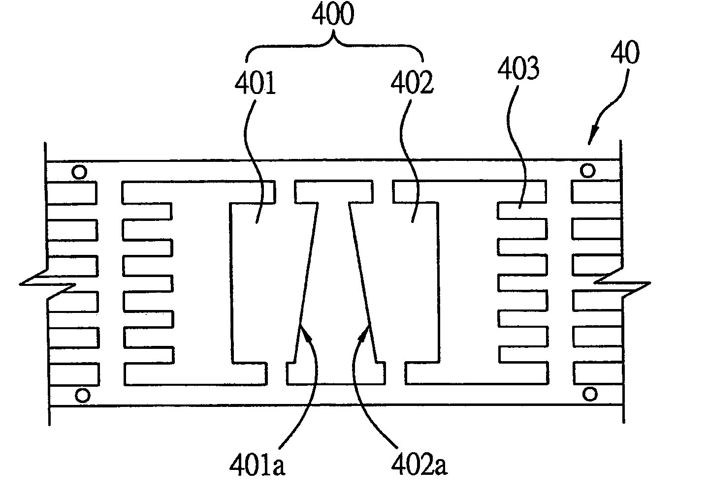
[0026]FIG. 4 is a top view of a lead frame structure 40 according to the present invention. The lead frame structure 40 (hereinafter also referred to as “lead frame 40”) comprises a die pad 400 and a plurality of leads 403 positioned around the die pad 400. The die pad 400 comprises a first mounting portion 401 and a second mounting portion 402 separated from the first mounting portion 401 by a gap. The first mounting portion 401 is formed with a blocking surface 401a bordering the gap, and the second mounting portion 402 is also formed with a blocking surface 402a bordering the gap, wherein...


PUM


Abstract

A lead frame structure is provided, which includes a die pad having a first mounting portion and a second mounting portion separated from the first mounting portion by a gap. The first and second mounting portions are formed with corresponding blocking surfaces bordering the gap, so as to allow a flow rate of an encapsulating resin flowing through the gap during a molding process to be reduced by the blocking surfaces, such that different portions of the encapsulating resin respectively flowing above, in and below the die pad can have substantially the same flow rate, thereby preventing bonding wires from being deformed to cause short circuit and avoiding formation of voids. A semiconductor package with the lead frame structure is also provided.

Description

FIELD OF THE INVENTION [0001] The present invention relates to lead frame structures and semiconductor packages integrated with the lead frame structures, and more particularly, to a lead frame structure having a separated die pad, and a semiconductor package integrated with the lead frame structure. BACKGROUND OF THE INVENTION [0002] In view of the increasing demands for electronic products that have miniaturized profiles and are capable of operating at high speeds, it is considered necessary to improve the performance and capacity of a single semiconductor package for use in a miniaturized electronic product. Accordingly, the single semiconductor package is intended to incorporate two or more semiconductor chips to form a multi-chip module with desirably reduced overall circuit size and enhanced electrical functionality. [0003]FIG. 1 shows a multi-chip semiconductor package disclosed in U.S. Pat. No. 5,793,108. This semiconductor package comprises a lead frame 10 having a die pad ...

Claims


Application Information

Patent Timeline
Patent Type & Authority Applications(United States)
IPC IPC(8): H01L21/00H01L23/495
CPCH01L21/565H01L23/49503H01L23/49575H01L2224/48091H01L2224/48247H01L2924/1532H01L2924/07802H01L24/48H01L2924/00014H01L2924/00H01L2924/181H01L2224/32145H01L2224/4826H01L2224/73215H01L2224/73265H01L2924/00012H01L2224/45099H01L2224/45015H01L2924/207
Inventor TSAI, WEN-SHANWEI, CHIEN-FENGLIU, HUNG-WENLIN, M.C.CHIANG, LIEN-CHEN
Owner SILICONWARE PRECISION IND CO LTD
Why Eureka
Try Eureka