Method and apparatus for attaching solder balls to substrate

a technology of substrate and solder ball, which is applied in the direction of printed circuit manufacturing, printed circuit aspects, solid-state devices, etc., can solve the problems of difficult detection, inoperable assembled flip chip devices and/or circuit boards, and electrical shorts, so as to increase yields above current levels, reduce substrate/package warping, and avoid the effect of reducing or eliminating the effect of warping

Inactive Publication Date: 2007-05-17
TEXAS INSTR INC
View PDF11 Cites 23 Cited by
  • Summary
  • Abstract
  • Description
  • Claims
  • Application Information

AI Technical Summary

Benefits of technology

[0012] According to one aspect of the invention, one method of applying the solder paste with distributed solder particles to the solder ball and the substrate solder pad comprises applying a solder paste with solder particles to the SOP pads utilizing a screening process. According to yet another aspect of the invention, another method of applying the solder paste to the solder balls is by dipping the solder balls into a layer of solder paste with distributed solder particles. The solder paste and solder particles are approximately uniformly dispersed throughout the paste. Another aspect of the invention is that the solder paste with distributed solder particles stabilize the solder balls so that when the substrate with solder balls is moved, prior to reflow, the ball do not move significantly or fall off the substrate, thus increasing yields over current technology.
[0013] According to yet ano...

Problems solved by technology

A typical concern with surface mounting flip chip packages to circuit boards is that electrical shorts can occur if the solder from adjacent contacts reflow together.
This shorting problem arises and is difficult to detect during the manufacturing process.
In addition, conductive solder paste on a circuit board can create a short that renders the assembled flip chip device and/or circuit board inoperable.
There is a greater likelihood of shorts occurring in these high density devices with high density grid patterns, because the spacing between adjacent contacts is very tight.
The electrical short is most easily detected after the assembly has been manufactured, and the problem often arises after the manufacturer has sold the electronic device.
There are numerous problems associated with detecting shorting issues after sale of the device.
For example, these devices often go into much larger electronic packages or devices, and therefore when a component fails the entire product ...

Method used


Image

  • Method and apparatus for attaching solder balls to substrate
  • Method and apparatus for attaching solder balls to substrate
  • Method and apparatus for attaching solder balls to substrate

Examples


Embodiment Construction

[0029] The present invention will now be described with reference to the drawings wherein like reference numerals are used to refer to like elements throughout. The present invention provides a method for attaching solder balls to a substrate. However, it will be appreciated that the invention may be advantageously employed in applications other than those illustrated and described herein. The drawings / figures are illustrations that are not drawn to scale.

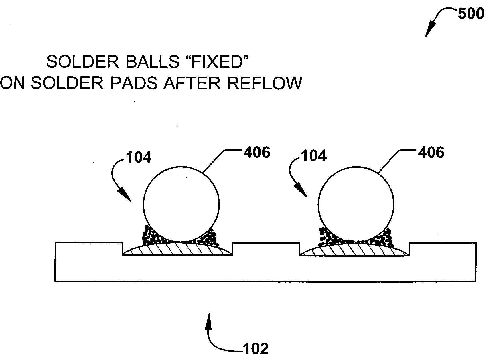
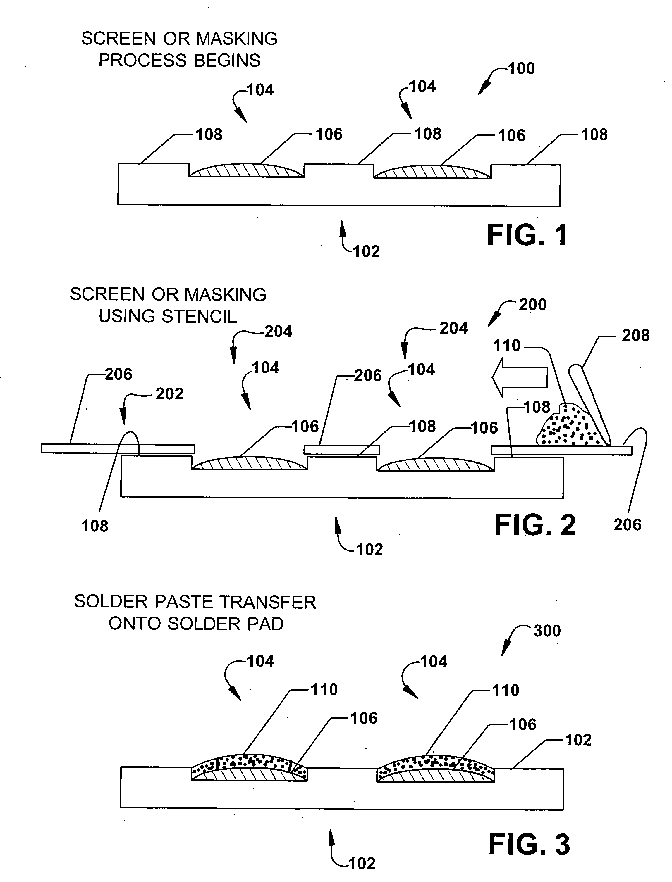
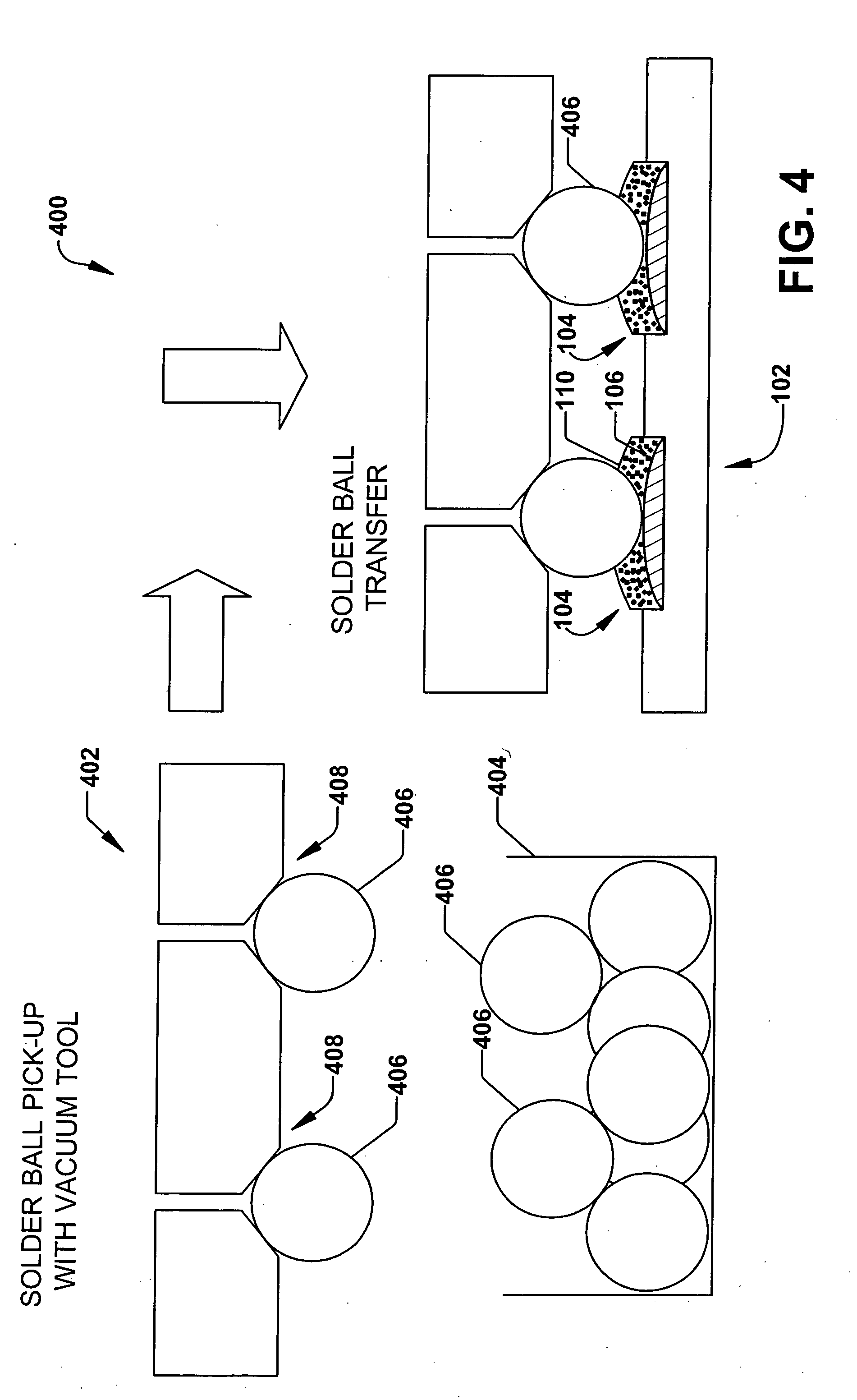
[0030] Referring now to the drawings, FIG. 1 through FIG. 5 illustrate a screen printing process that utilizes solder paste mixed with solder particles to position the solder ball accurately prior to a reflow process. In FIG. 1, a substrate 102 with SOP (solder on pad) pads 104 is illustrated. The SOP pads 104 are shown recessed into the substrate 102 where the upper surface of the convex pad face 106 is level with the upper surface of the substrate 108, for example. The SOP pads 104 can include at least one of the following mater...


PUM


Abstract

A method for attaching solder balls to solder pads on a circuit board, comprising distributing an approximately uniform flat layer of solder paste with distributed solder particles on top of a flat plate employing a squeegee, picking up the solder balls from a solder ball bin utilizing a vacuum tool, dipping the solder balls into the solder paste, lifting the solder balls out of the solder paste, placing the solder balls with the solder paste proximate to the center of the solder pad, releasing the solder balls, and reflowing assembly comprising the substrate, the solder balls, the solder paste, and solder particles in a reflow oven.

Description

RELATED APPLICATION [0001] This application claims priority to U.S. Provisional Application Ser. No. 60 / 732,503, filed Nov. 1, 2005, entitled “METHOD AND APPARATUS FOR ATTACHING SOLDER BALLS TO SUBSTRATE”.FIELD OF THE INVENTION [0002] The present invention relates generally to solder balls on substrates and more particularly to an improved system and method for attaching solder balls to substrates utilizing solder paste with distributed solder particles. BACKGROUND OF THE INVENTION [0003] Packaged microelectronic memory devices, for example, are used in laptop computers, PDAs, scanners, cell phones, and the like. One approach used today is flip chip interconnect technology for electrically connecting the silicon die directly to the package carrier. The package carrier, either a substrate or leadframe, provides the connection from the silicon die to the exterior of the package. In standard packaging, the interconnection between the silicon die and the carrier is typically made using ...

Claims


Application Information

Patent Timeline
IPC IPC(8): H01L21/44
CPCH01L21/4853H01L24/11H01L24/12H01L2224/13099H01L2924/01029H01L2924/01047H01L2924/01079H01L2924/01082H01L2924/30107H05K1/111H05K3/3478H05K3/3484H05K2201/035H05K2201/098H05K2201/10992H05K2203/0338H05K2203/041H05K2203/043H01L2224/11003H01L2224/1132H01L2224/11334H01L2224/742H01L2924/01033H01L2924/014H01L2224/1131H01L2224/11822H01L2924/10253H01L2924/00H05K3/3485
Inventor COWENS, MARVIN W.BAYOT, ARTHUR A.AREOLA, JABEEHMARTINEZ, SERGIO
Owner TEXAS INSTR INC
Why Eureka
Try Eureka