Interconnect structure and fabricating method thereof

a technology of interconnection structure and fabrication method, which is applied in the direction of semiconductor devices, semiconductor/solid-state device details, electrical apparatus, etc., can solve the problems of reducing the reliability of the device and the yield of the product, reducing the length of the process line, and few problems, so as to improve the reliability of the device and the product yield

Active Publication Date: 2007-05-24
UNITED MICROELECTRONICS CORP
View PDF9 Cites 24 Cited by
  • Summary
  • Abstract
  • Description
  • Claims
  • Application Information

AI Technical Summary

Benefits of technology

[0006] Accordingly, this invention provides an interconnect structure capable of solving the high aspect ratio issues to improve the device reliability and the product yield.

Problems solved by technology

With the rapid development in the IC industry, the integration degree of semiconductor devices is always required higher so that the IC process linewidth is decreased unceasingly.
This is due to the high aspect ratio of the via / contact hole, and results in quite a few problems.
Consequently, some dielectric material easily remains at the bottom of the contact hole 145 to cause a high contact resistance or even an open circuit and a void defect easily forms in the subsequent conductor gap-filling process, so that the reliability of the device and the yield of the product are lowered.

Method used


Image

  • Interconnect structure and fabricating method thereof
  • Interconnect structure and fabricating method thereof
  • Interconnect structure and fabricating method thereof

Examples


Embodiment Construction

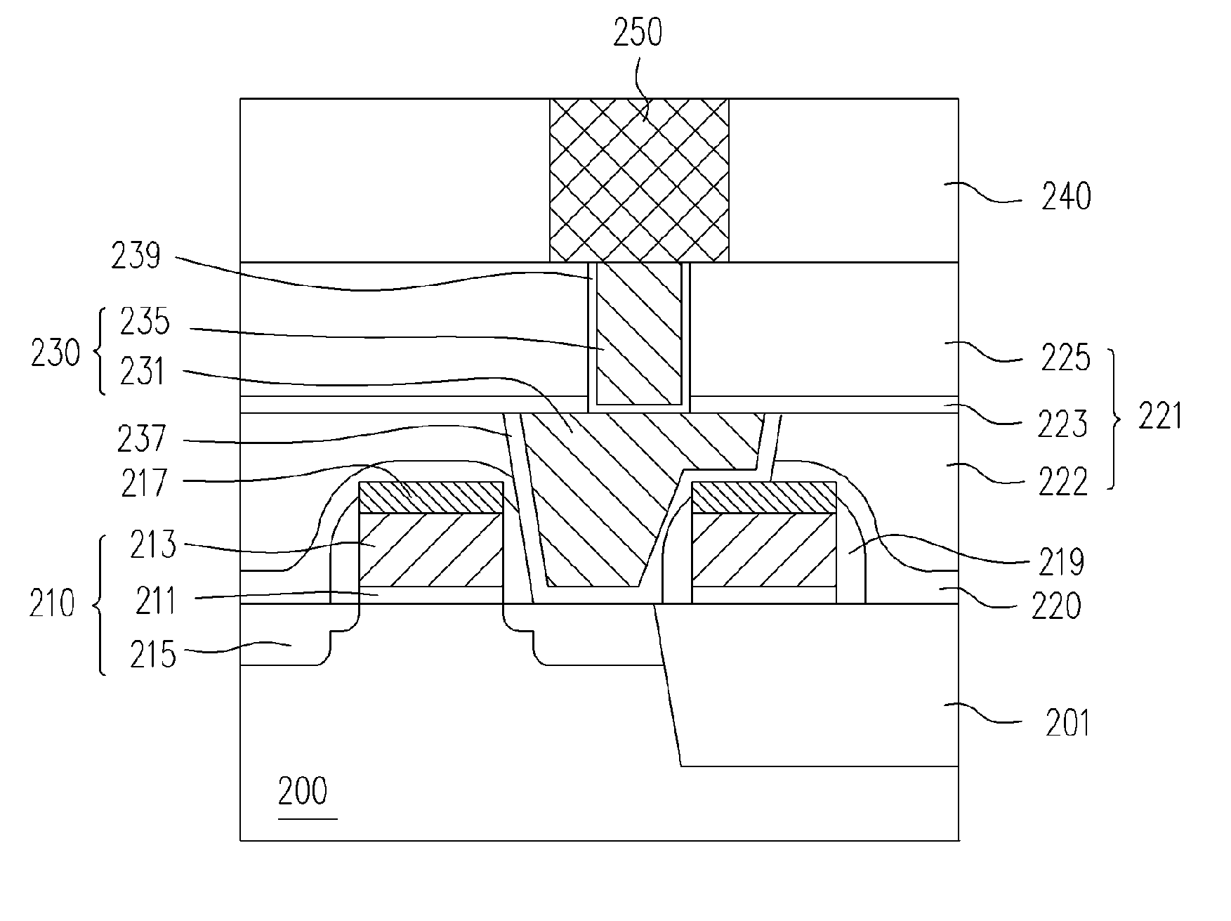
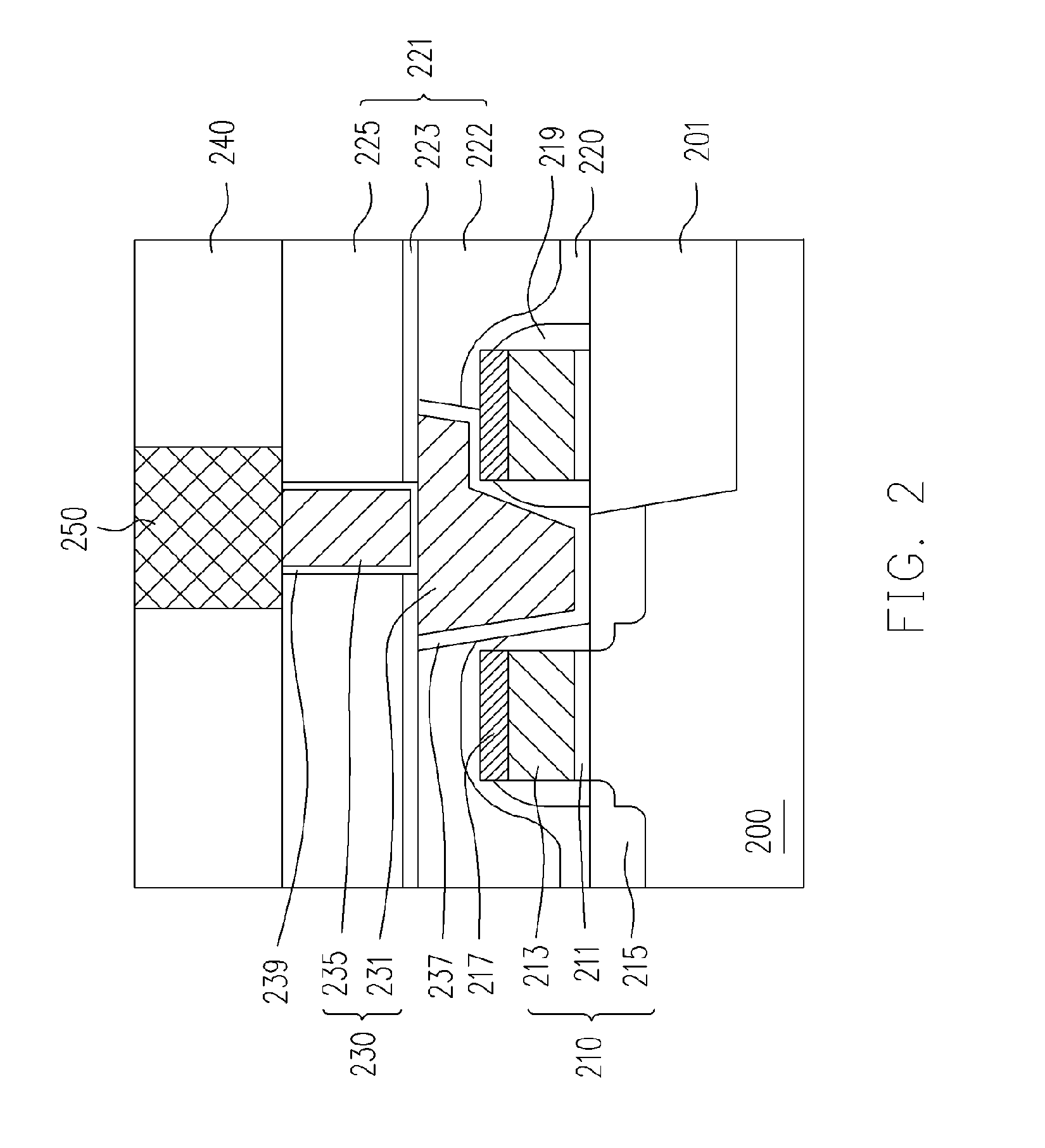
[0021] Referring to FIG. 2, the interconnect structure of the embodiment is disposed on a substrate 200 having an isolation structure 201 and multiple semiconductor devices 210 thereon. Each device 210 may be a MOS transistor including gate dielectric 211 on the substrate 200, a gate 213 on the gate dielectric 211, and S / D regions 215 in the substrate 200 beside the gate 213, wherein the gate dielectric 211 may include SiO, the gate 213 includes a conductive material like doped polysilicon or metal, and the S / D regions 215 are p+-doped or n+-doped. A metal silicide layer 217 including TiSi, CoSi, NiSi or PtSi may be further disposed on the gate 213, and the sidewall of the gate 213 may be further disposed with a spacer 219 possibly composed of SiN. An etching stop layer 220, such as a SiN layer, may be further disposed on the devices 210.

[0022] The aforementioned structure is covered by a dielectric layer 221, in which a composite plug 230 is disposed electrically connecting with a...


PUM


Abstract

An interconnect structure is described, disposed on a substrate with a conductive part thereon and including a dielectric layer, a composite plug and a conductive line. The dielectric layer is disposed on the substrate covering the conductive part. The composite plug is disposed in the dielectric layer electrically connecting with the conductive part, and includes a first plug and a second plug on the first plug, wherein the material or the critical dimension of the second plug is different from that of the first plug. The conductive line is disposed on the dielectric layer electrically connecting with the composite plug.

Description

BACKGROUND OF THE INVENTION [0001] 1. Field of the Invention [0002] The present invention relates to an integrated circuit structure and fabrication thereof. More particularly, the present invention relates to an interconnect structure, and to a method for fabricating the same. [0003] 2. Description of the Related Art [0004] With the rapid development in the IC industry, the integration degree of semiconductor devices is always required higher so that the IC process linewidth is decreased unceasingly. Hence, the process window of a back-end interconnect process is decreased rapidly, especially when a via / contact hole is to be formed. This is due to the high aspect ratio of the via / contact hole, and results in quite a few problems. [0005]FIG. 1 illustrates a cross-sectional view of a conventional contact plug of MOS transistor. The contact plug 150 is disposed between two MOS transistors 110 and 120 electrically connecting with a shared source / drain (S / D) region 130, wherein the MOS ...

Claims


Application Information

Patent Timeline
Patent Type & Authority Applications(United States)
IPC IPC(8): H01L23/48H01L21/4763
CPCH01L21/76807H01L21/76838H01L21/76895H01L23/5226H01L23/53223H01L23/53238H01L23/53252H01L23/5329H01L23/53295H01L2924/0002
Inventor HSU, YU-HAOCHEN, MING-TSUNG
Owner UNITED MICROELECTRONICS CORP
Why Eureka
Try Eureka