Multilayer circuit with variable inductor, and method of manufacturing it

a technology of variable inductance and multilayer circuit, which is applied in the direction of semiconductor devices, basic electric elements, semiconductor/solid-state device details, etc., can solve the problems of difficult integration of variable inductance into integrated circuits, complicated manufacture of variable inductors, and need for additional power-consuming control circuits

Inactive Publication Date: 2007-05-24
SEIKO EPSON CORP
View PDF4 Cites 33 Cited by
  • Summary
  • Abstract
  • Description
  • Claims
  • Application Information

AI Technical Summary

Problems solved by technology

However, a problem involved with this kind of variable inductors based on MEMS involving moveable elements (like the above-mentioned dielectric sheet) is that their manufacture can be rather complex and expensive, and that it may be difficult to integrate them in integrated circuits, using standard IC processes (such as CMOS processes) for their manufacture.
However, a problem involved with this kind of arrangements is that an additional power-consuming control circuit is needed, which not only implies an extra amount of circuitry, but also additional power consumption, which can be inconvenient and even critical when it comes to the design of low power consumption integrated circuits.
This arrangement can easily be integrated into integrated circuits using standard IC processes (such as CMOS, etc.), but it may not be optimal when it comes to the issues of parasitic capacitance and quality factor.
The stacked inductors can give rise to an additional capacitance between them, which can cause, for example, a reduction of the self-resonant frequency of the inductor, making it unsuitable for certain high frequency applications.
Also, the disclosed arrangement may not be optimal in what concerns the quality factor; it may provide a rather low quality factor, especially in IC arrangements optimized for radio frequency (RF) applications.

Method used


Image

  • Multilayer circuit with variable inductor, and method of manufacturing it
  • Multilayer circuit with variable inductor, and method of manufacturing it
  • Multilayer circuit with variable inductor, and method of manufacturing it

Examples


Embodiment Construction

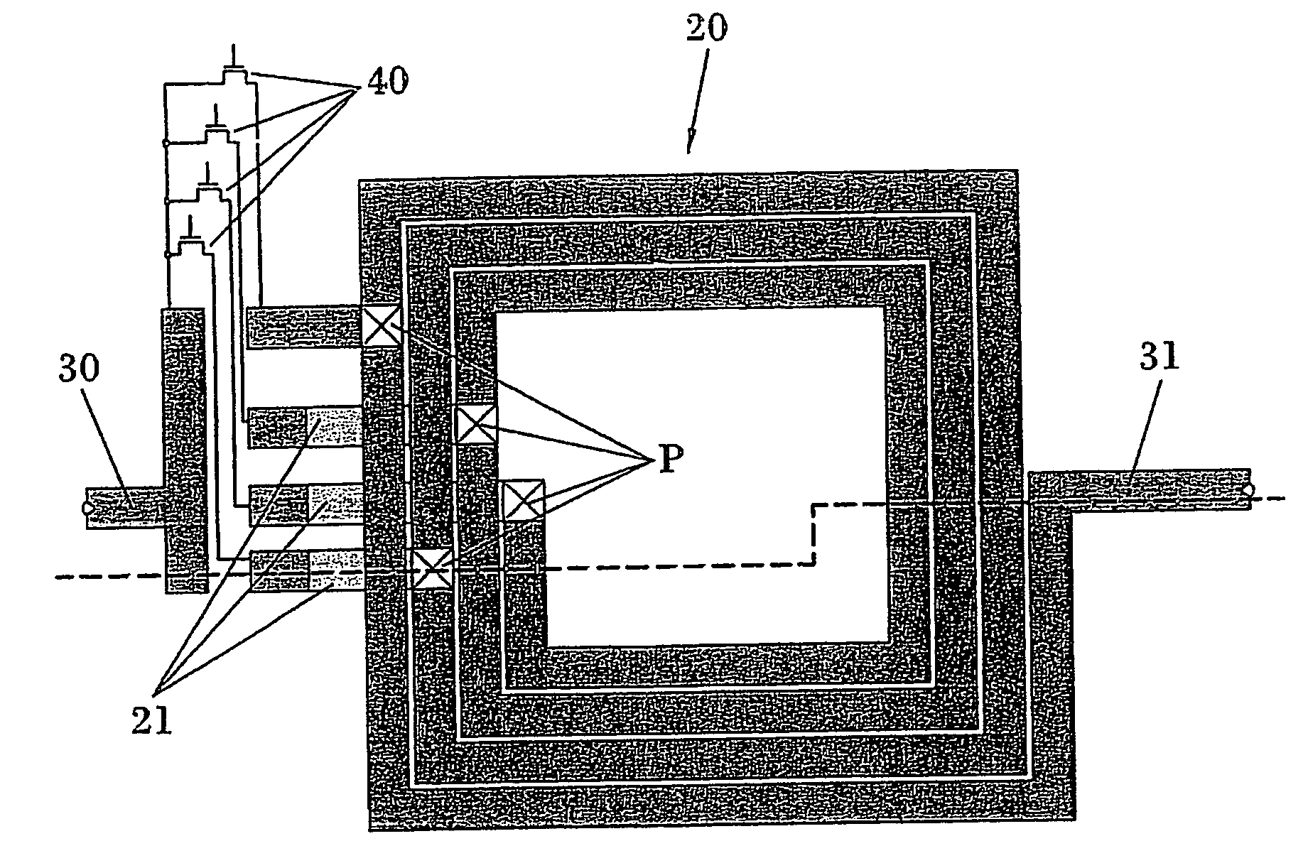
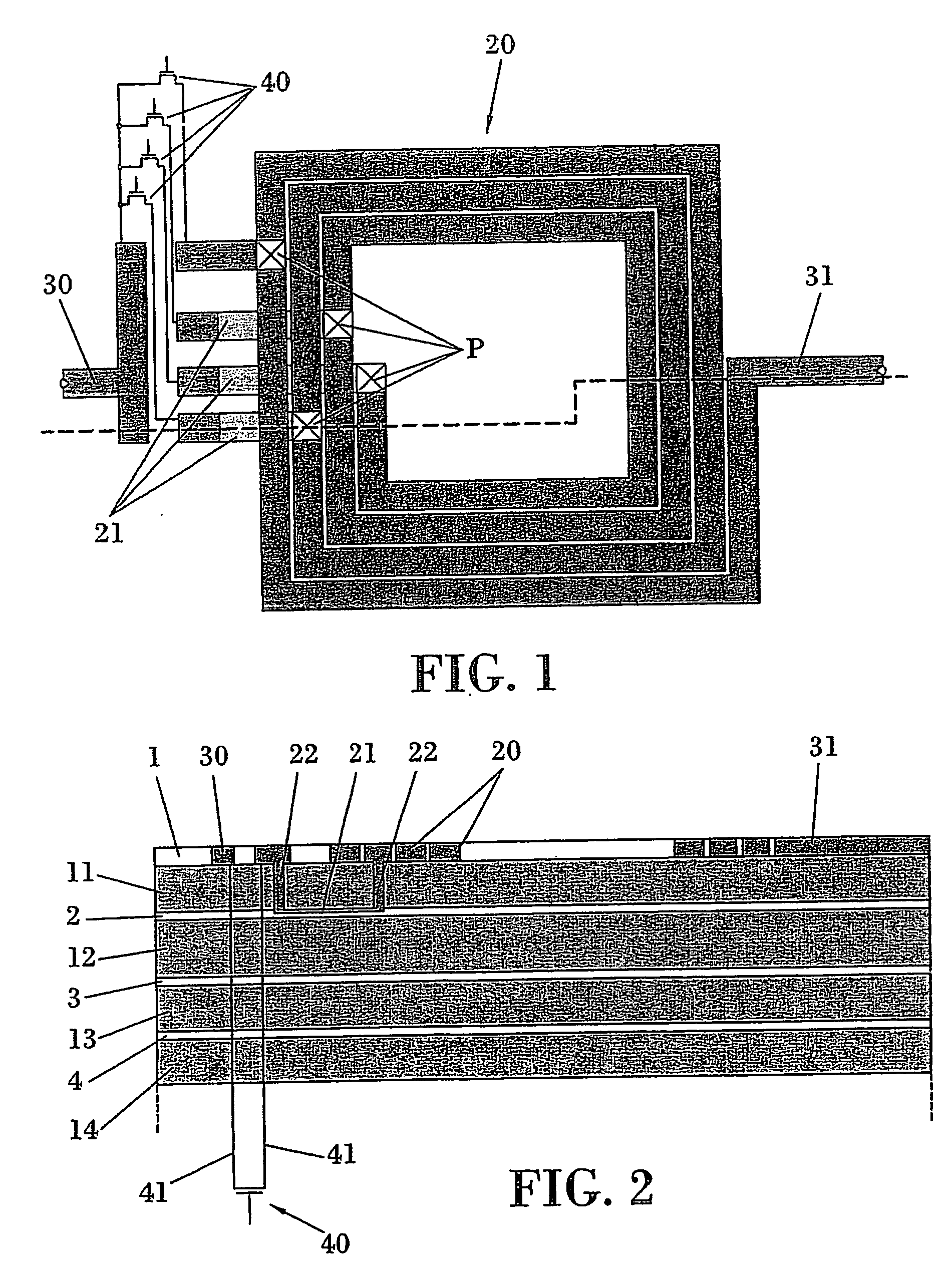
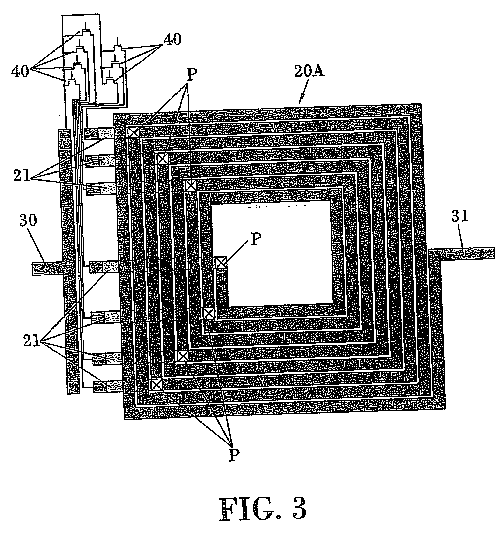
[0010] A first aspect of the invention relates to a multilayer structure or circuit comprising a plurality of electrically conductive layers (such as metal layers) separated from each other by respective insulating or dielectric layers, wherein said multilayer circuit comprises at least one variable inductor. According to the invention, the variable inductor comprises

[0011] a conductive coil structure following a coil path in a single one of said conductive layers,

[0012] two ports connected (or “connectable”, through corresponding switches) to said coil structure, and

[0013] a switch arrangement, comprising at least one switch, for selectively connecting at least one of said ports to one of a plurality of specific positions of said coil structure along said coil path, thus providing for a corresponding selective inductance value of the variable inductor, between said two ports.

[0014] According to the invention, the coil structure is arranged in the thickest one of said conductive...


PUM

PropertyMeasurementUnit
frequencyaaaaaaaaaa
frequencyaaaaaaaaaa
electrically conductiveaaaaaaaaaa

Abstract

The multilayer circuit comprising a plurality of electrically conductive layers separated from each other by respective dielectric layers, wherein at least one variable inductor is provided that comprises: a conductive coil structure following a coil path in a single and thickest one of said conductive layers; two ports connected to said coil structure; and a switch arrangement comprising at least one switch for selectively connecting at least one of said ports to one of a plurality of specific positions of said coil structure along said coil path in said one of said conductive layers, thus providing for a corresponding selective inductance value of the variable inductor, between said two ports. The invention also relates to a method of manufacturing the circuit.

Description

FIELD OF THE INVENTION [0001] The invention relates to the field of variable inductors in microelectronic circuits, such as silicon based integrated circuits having a plurality of metal layers separated by dielectric layers. STATE OF THE ART [0002] Variable passive devices are frequently used in electronic circuits; for example, in many analog and radio frequency (RF) circuits, there is a need to use some reactive components such as capacitors and inductors. Some examples of circuits in which such devices are used are filters, Voltage Controlled Oscillators (VCO), impedance matching networks, and others. In order to provide such circuits with the possibility of some degree of tuning, it is known to use variable capacitors and inductors, that is, capacitors and inductors the values of which can be varied to a certain extent. One very well known example of such a variable component is the so-called varicap diode, which allows a certain variability of the capacitance value by means of ...

Claims


Application Information

Patent Timeline
Patent Type & Authority Applications(United States)
IPC IPC(8): H01F5/00
CPCH01F21/12H01L23/5227H01L2924/3011H01L2924/0002H01L2924/00H01L27/04H01L23/64
Inventor CAIRO MOLINS, JOSEP IGNASI
Owner SEIKO EPSON CORP
Why Eureka
Try Eureka