
Eureka
For R&D, Eureka makes reading and utilizing patents & technical documents easy.
Eureka AIR
Designed for self-driven R&D workflows. Generate viable solutions, solve complex R&D challenges, empower your innovation with AI.

Eureka Materials
Designed for material experts only. Revolutionize your material R&D, from search, analyze, to developing new materials.

TechResearch
Generate reliable direction feasibility study reports for your R&D in just a few steps.

TechSeek
Discover and master advanced knowledge NOW. Basics, ideas, possibilities, all at once.

TechMind
As an expert in R&D Theories, TechMind can generates customized viable solutions instantly.

TechRisk
Analyze your overall solution with one click, know your potential R&D risks in advance.

TechMonitor
Get weekly tech updates, stay abreast of the latest tech innovations and key insights.
Assembly jig and manufacturing method of multilayer semiconductor device
- Summary
- Abstract
- Description
- Claims
- Application Information
AI Technical Summary
Benefits of technology
Problems solved by technology
Method used
Image

Examples
Embodiment Construction
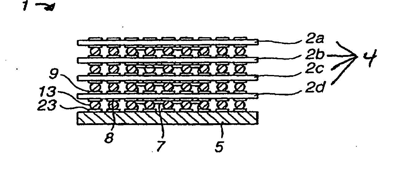
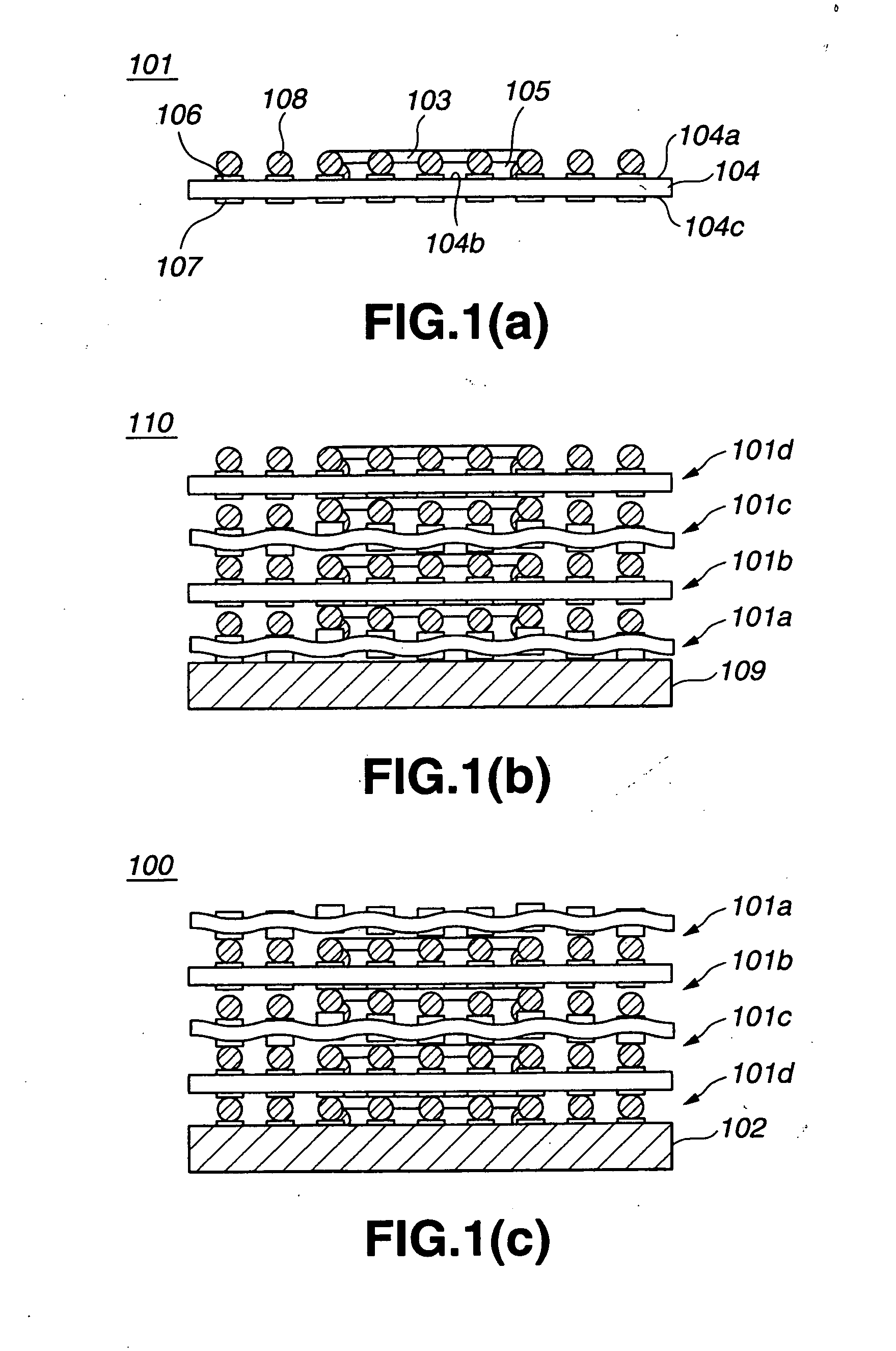
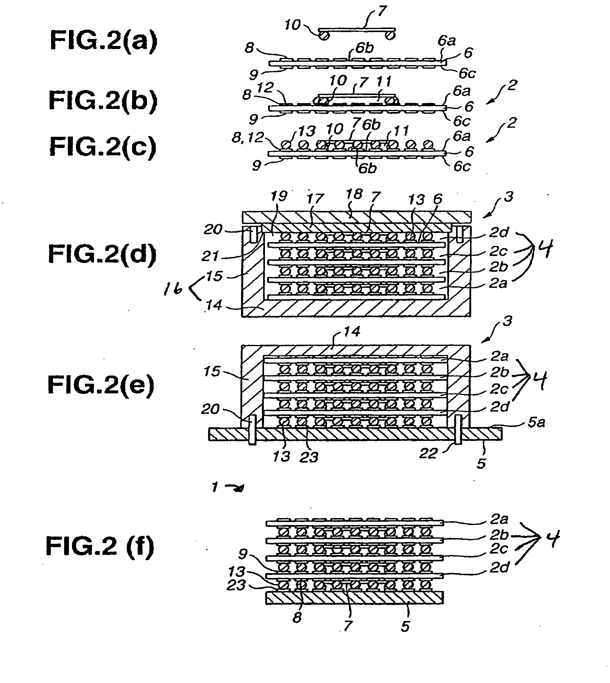
[0030] Embodiments of the present invention will be described in further detail with reference to the accompanying drawings. Manufacturing processes for the multilayer semiconductor device 1 according to the embodiment are almost the same as those for the above-mentioned conventional multilayer semiconductor device 100. As shown in FIG. 2, the multilayer semiconductor device 1 in FIG. 2 (f) is manufactured through the following processes. Namely, a semiconductor module 2 is manufactured. A layered semiconductor module unit 4 is manufactured by layering many semiconductor modules 2 (2a to 2d) through the use of a assembly jig 3. Finally, the layered semiconductor module unit 4 is mounted on a mother substrate 5 through the use of a assembly jig 3.
[0031] The manufacturing processes for the semiconductor module 2 include a process of mounting a semiconductor chip 7 on a printed-wiring board 6 as a first process. As regards the printed-wiring board 6, a photographic technique or the li...
PUM
 Abstract
Description
Claims
Application Information
 - R&D Engineer
- R&D Manager
- IP Professional
- Industry Leading Data Capabilities
- Powerful AI technology
- Patent DNA Extraction
Browse by: Latest US Patents, China's latest patents, Technical Efficacy Thesaurus, Application Domain, Technology Topic, Popular Technical Reports.
© 2024 PatSnap. All rights reserved.Legal|Privacy policy|Modern Slavery Act Transparency Statement|Sitemap|About US| Contact US: help@patsnap.com