
Compact static memory cell with non-volatile storage capability

Active Publication Date: 2007-05-31
SYNOPSYS INC
View PDF9 Cites 13 Cited by
  • Summary
  • Abstract
  • Description
  • Claims
  • Application Information

AI Technical Summary

Benefits of technology

[0013] Conventional SRAM cells provide high-speed data access, but are unable to retain stored data once power is removed. Adding floating gate transistors to such SRAM cells can provide non-volatile data storage behavior, but at the cost of increasing overall cell size and fabrication process complexity. However, by incorporating programmable resistors into layers above (or below) SRAM cells (e.g., metallization layers), non-volatile capabilities can be provided without increasing cell layout size.
[0019] In one embodiment, the SRAM data storage structure can be “weakened” during this startup procedure to improve the voltage pulldown performance when restoring a logic LOW voltage to the SRAM data storage structure. For example, the NDR transistors in the 3T transistor circuit will generally require a high gate bias voltage (i.e., greater than the logic HIGH voltage plus the NDR transistor threshold voltage) to ensure proper latching operation. During the startup operation, this gate bias voltage can be reduced, thereby weakening the latching effect provided by the NDR transistors so that the logic HIGH voltage at the storage node is more easily pulled down to the logic LOW voltage (when necessary). In another embodiment, if the SRAM data storage structure is a 6T SRAM circuit, the upper supply voltage provided to the circuit during the startup operation can be reduced to provide a similar “latch weakening” effect.
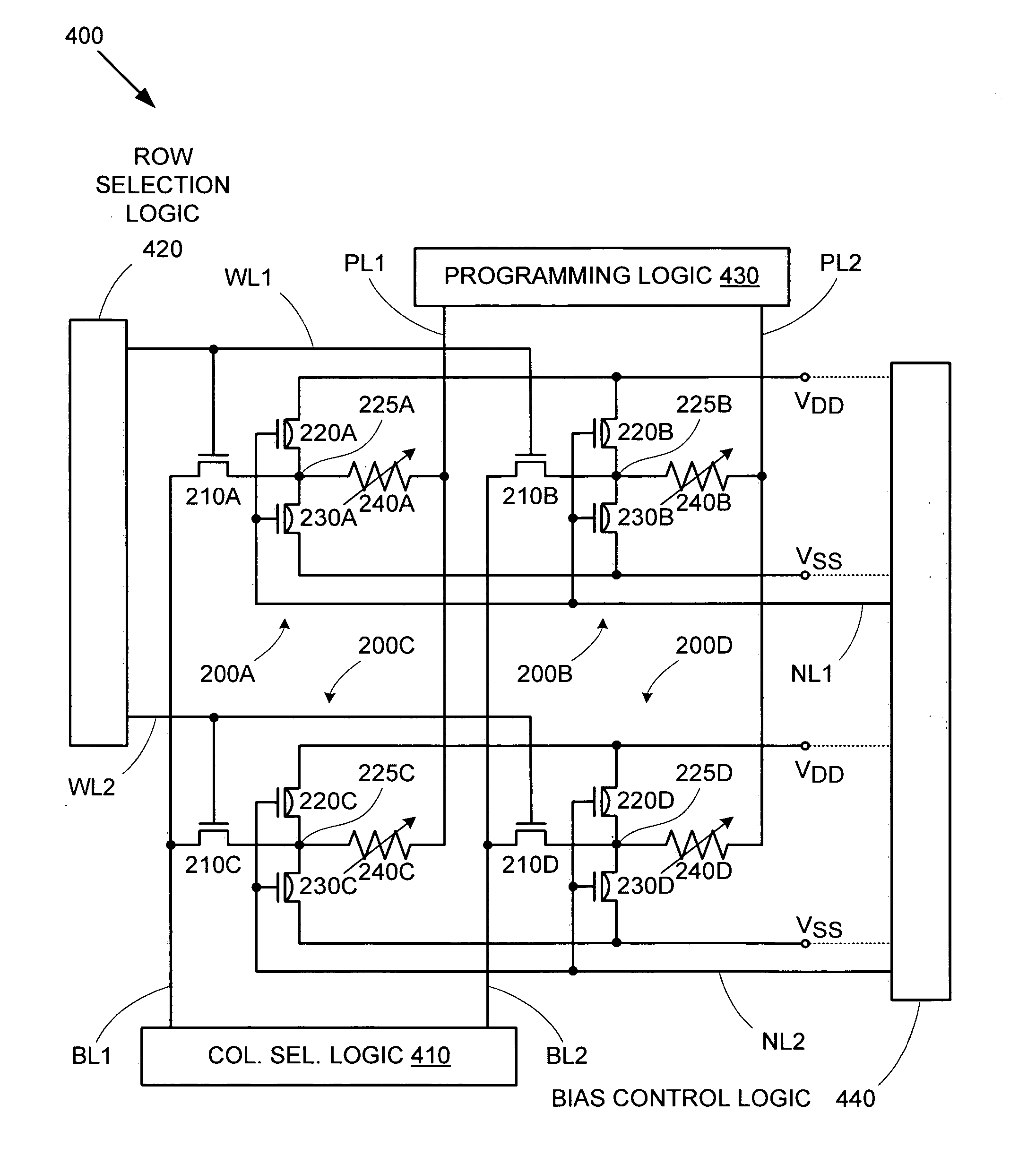
[0020] In another embodiment, a memory array can include an array of SRAM cells, each including a programmable resistor connected to a storage node of the SRAM cell. During a shutdown procedure for the memory array, the data stored in the SRAM cells can be “transferred” to the programmable resistors (e.g., if a particular SRAM cell is storing a logic HIGH voltage, the programmable resistor connected to that SRAM cell can be maintained at a high resistance state, while if the SRAM cell stores a logic LOW voltage, the programmable resistor can be programmed to a low resistance state). During a startup procedure for the memory array, appropriate data values can be written back in to the SRAM cells based on the (resistance) states of the programmable resistors. Therefore, during normal operation of the memory array, the high performance benefits of the SRAM cells can be realized, while the programmable resistors allow the memory array to retain stored data even when power is removed from the memory array.

Problems solved by technology

Conventional SRAM cells provide high-speed data access, but are unable to retain stored data once power is removed.
Adding floating gate transistors to such SRAM cells can provide non-volatile data storage behavior, but at the cost of increasing overall cell size and fabrication process complexity.

Method used


Image

  • Compact static memory cell with non-volatile storage capability
  • Compact static memory cell with non-volatile storage capability
  • Compact static memory cell with non-volatile storage capability

Examples


Embodiment Construction

[0027] Conventional SRAM cells provide high-speed data access, but are unable to retain stored data once power is removed. Adding floating gate transistors to such SRAM cells can provide non-volatile data storage behavior, but at the cost of increasing overall cell size and fabrication process complexity. However, by incorporating programmable resistors into layers above (or below) SRAM cells (e.g., metallization layers), non-volatile storage capability can be provided without increasing cell layout size.

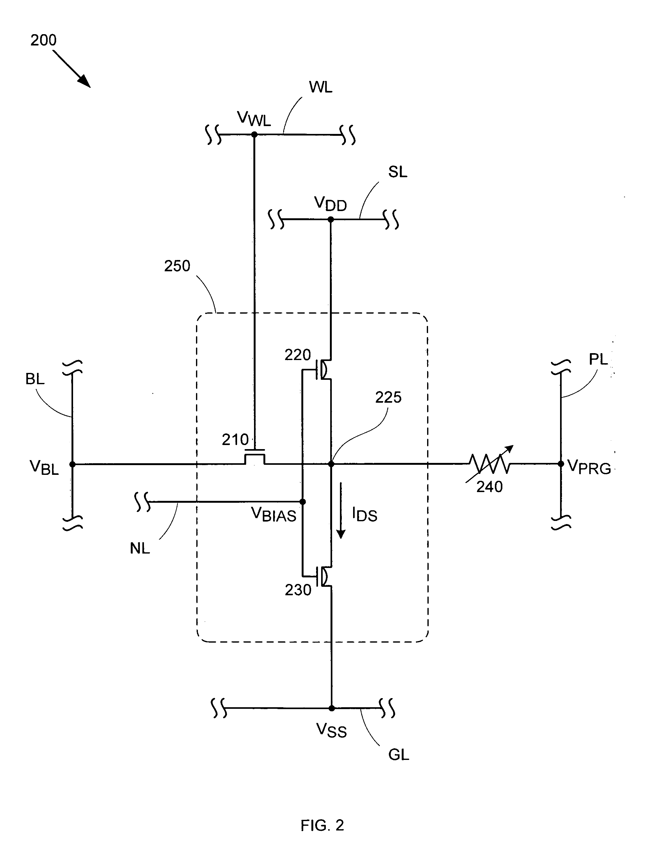
[0028]FIG. 2 shows a schematic circuit diagram of an embodiment of a non-volatile SRAM cell 200. Non-volatile SRAM cell 200 includes an SRAM circuit 250 and a programmable resistor 240. Programmable resistor 240 is connected between a program line PL and a (data) storage node 225 in SRAM circuit 250. Note that for exemplary purposes, SRAM circuit 250 is depicted as a “3T” SRAM cell that includes n-channel transistors 210, 220, and 230. However, according to various other embodiment...


PUM


Abstract

A static random access memory (SRAM) cell includes a SRAM circuit and a programmable resistor connected to a storage node of the SRAM circuit. The SRAM circuit can be any type of SRAM circuit, such as a 3T, negative differential resistance (NDR) transistor-based circuit, or a 6T (conventional SRAM) circuit. The programmable resistor can be formed in a metal layer above the SRAM circuit to minimize the area requirements for the memory cell. Just before shutdown of the SRAM cell, the resistance state of the programmable resistor is changed (if necessary) based on the data value stored at the storage node. The programmable resistor provides a non-volatile indication of the stored data value at the time of power off. Then, when power is restored to the SRAM cell, a data value based on the resistance state of the programmable resistor is written back into the SRAM circuit.

Description

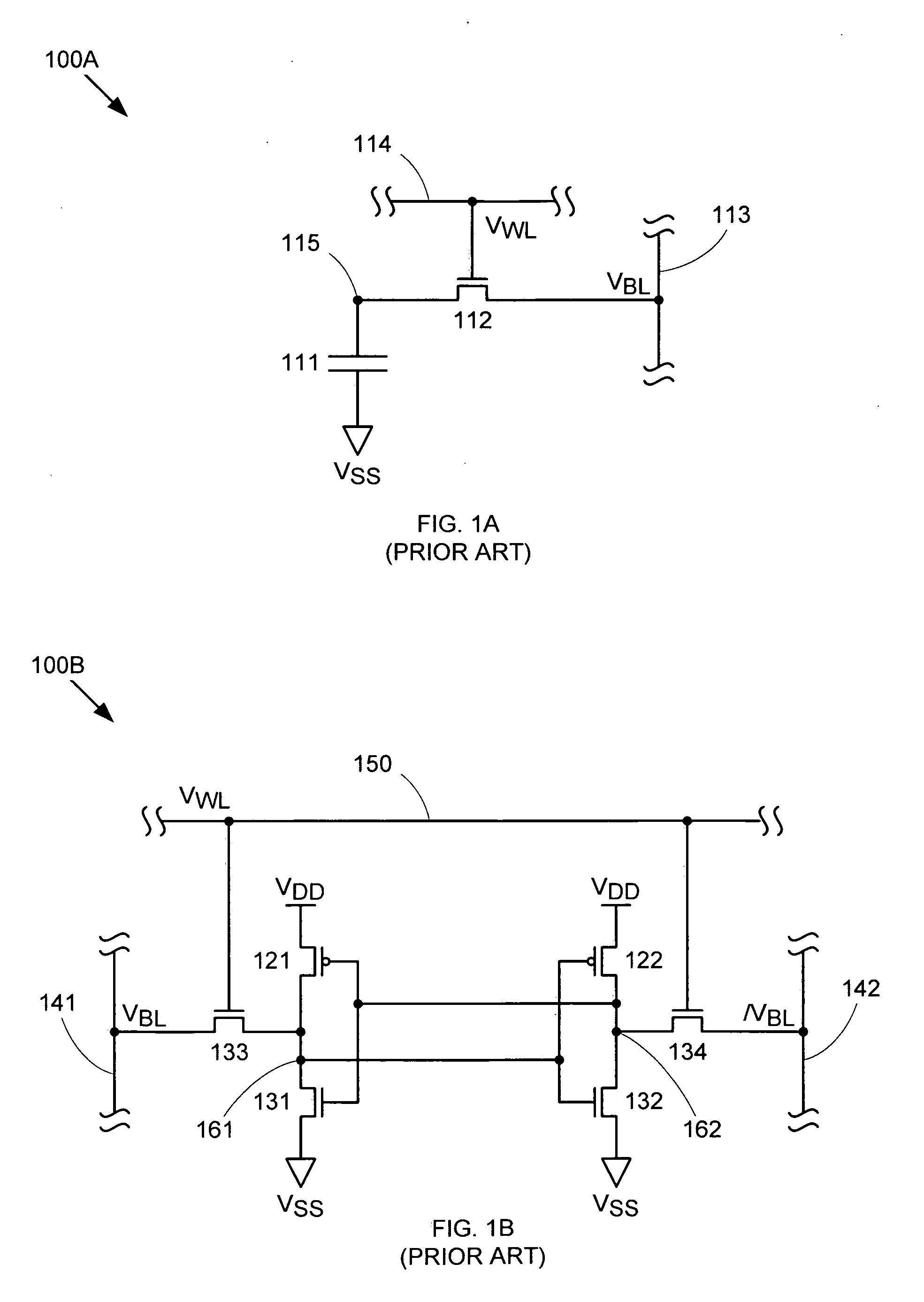
BACKGROUND OF THE INVENTION [0001] 1. Field of the Invention [0002] The invention relates to the field of semiconductor memory, and in particular, to a structure and method for providing non-volatile data storage in high-speed memory. [0003] 2. Related Art [0004] Random access memory (RAM) is memory used in electronic device applications that provides direct access to stored data. The two main types of RAM are dynamic random access memory (DRAM) and static random access memory (SRAM). A schematic circuit diagram of a DRAM cell 100A is depicted in FIG. 1A. DRAM cell 100A includes a storage capacitor 111 and an access transistor 112. Access transistor 112 is connected between a bit line 113 and storage capacitor 111, and the gate of access transistor 112 is connected to a word line 114. To write a data value into a storage node 115 at a junction between storage capacitor 111 and access transistor 112, bit line 113 is set to the appropriate data level, and word line 114 is set to a log...

Claims


Application Information

Patent Timeline
IPC IPC(8): G11C11/00
CPCG11C11/005G11C13/0011G11C14/009
Inventor KING, TSU-JAE
Owner SYNOPSYS INC
Learn More